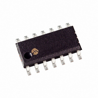
PIC16F630-I/SL Microchip Technology, PIC16F630-I/SL Datasheet - Page 70

PIC16F630-I/SL
Manufacturer Part Number
PIC16F630-I/SL
Description
IC MCU FLASH 1KX14 EEPROM 14SOIC
Manufacturer
Microchip Technology
Series
PIC® 16Fr
Datasheets
1.PIC16F616T-ISL.pdf
(8 pages)
2.PIC12F629T-ISN.pdf
(24 pages)
3.PIC16F630-ISL.pdf
(132 pages)
4.PIC16F630-ISL.pdf
(2 pages)
5.PIC16F630-ISL.pdf
(10 pages)
6.PIC16F676-EP.pdf
(132 pages)
7.PIC16F676-ISL.pdf
(130 pages)
Specifications of PIC16F630-I/SL
Program Memory Type
FLASH
Program Memory Size
1.75KB (1K x 14)
Package / Case
14-SOIC (3.9mm Width), 14-SOL
Core Processor
PIC
Core Size
8-Bit
Speed
20MHz
Peripherals
Brown-out Detect/Reset, POR, WDT
Number Of I /o
12
Eeprom Size
128 x 8
Ram Size
64 x 8
Voltage - Supply (vcc/vdd)
2 V ~ 5.5 V
Oscillator Type
Internal
Operating Temperature
-40°C ~ 85°C
Processor Series
PIC16F
Core
PIC
Data Bus Width
8 bit
Data Ram Size
64 B
Interface Type
RS- 232/USB
Maximum Clock Frequency
20 MHz
Number Of Programmable I/os
12
Number Of Timers
2
Operating Supply Voltage
2 V to 5.5 V
Maximum Operating Temperature
+ 85 C
Mounting Style
SMD/SMT
3rd Party Development Tools
52715-96, 52716-328, 52717-734
Development Tools By Supplier
PG164130, DV164035, DV244005, DV164005, PG164120, ICE2000, DM163014, DM164120-4
Minimum Operating Temperature
- 40 C
Package
14SOIC N
Device Core
PIC
Family Name
PIC16
Maximum Speed
20 MHz
Lead Free Status / RoHS Status
Lead free / RoHS Compliant
Data Converters
-
Connectivity
-
Lead Free Status / Rohs Status
Lead free / RoHS Compliant
Available stocks
Company
Part Number
Manufacturer
Quantity
Price
Company:
Part Number:
PIC16F630-I/SL
Manufacturer:
TriQuint
Quantity:
1 200
Company:
Part Number:
PIC16F630-I/SL
Manufacturer:
MICROCHI
Quantity:
1 743
Part Number:
PIC16F630-I/SL
Manufacturer:
MICROCHIP/微芯
Quantity:
20 000
PIC16F630/676
9.7
The Power-down mode is entered by executing a
SLEEP
If the Watchdog Timer is enabled:
• WDT will be cleared but keeps running
• PD bit in the STATUS register is cleared
• TO bit is set
• Oscillator driver is turned off
• I/O ports maintain the status they had before
For lowest current consumption in this mode, all I/O
pins should be either at V
circuitry drawing current from the I/O pin and the
comparators and CV
that are hi-impedance inputs should be pulled high or
low externally to avoid switching currents caused by
floating inputs. The T0CKI input should also be at V
or
contribution from on-chip pull-ups on PORTA should be
considered.
The MCLR pin must be at a logic high level (V
9.7.1
The device can wake-up from SLEEP through one of
the following events:
1.
2.
3.
FIGURE 9-13:
DS40039E-page 68
INSTRUCTION FLOW
(INTCON<1>)
SLEEP
hi-impedance).
Note:
(INTCON<7>)
Note
INTF flag
GIE bit
Instruction
Fetched
Instruction
Executed
CLKOUT
V
External RESET input on MCLR pin
Watchdog Timer Wake-up (if WDT was enabled)
Interrupt from RA2/INT pin, PORTA change, or
a peripheral interrupt.
SS
INT pin
instruction.
OSC1
1:
2:
3:
4:
Power-Down Mode (SLEEP)
PC
was executed (driving high, low, or
for
(4)
It should be noted that a RESET generated
by a WDT time-out does not drive MCLR
pin low.
WAKE-UP FROM SLEEP
XT, HS or LP Oscillator mode assumed.
T
delay in INTOSC mode.
GIE = '1' assumed. In this case after wake-up, the processor jumps to the interrupt routine. If GIE = '0', execution will continue in-line.
CLKOUT is not available in XT, HS, LP or EC Osc modes, but shown here for timing reference.
OST
Q1 Q2 Q3 Q4 Q1 Q2 Q3 Q4 Q1
Inst(PC) = SLEEP
lowest
= 1024T
Inst(PC - 1)
PC
REF
WAKE-UP FROM SLEEP THROUGH INTERRUPT
OSC
current
should be disabled. I/O pins
DD
(drawing not to scale). Approximately 1 μs delay for RC Oscillator mode. See Section 12 for wake-up from SLEEP
, or V
Inst(PC + 1)
SLEEP
PC+1
SS
consumption.
, with no external
Processor in
SLEEP
IHMC
PC+2
The
).
DD
T
OST
(2)
Q1 Q2 Q3 Q4 Q1 Q2 Q3 Q4 Q1 Q2 Q3 Q4 Q1 Q2 Q3 Q4
Interrupt Latency
Inst(PC + 2)
Inst(PC + 1)
The first event will cause a device RESET. The two
latter events are considered a continuation of program
execution. The TO and PD bits in the STATUS register
can be used to determine the cause of device RESET.
The PD bit, which is set on power-up, is cleared when
SLEEP is invoked. TO bit is cleared if WDT Wake-up
occurred.
When the
next instruction (PC + 1) is pre-fetched. For the device
to wake-up through an interrupt event, the correspond-
ing interrupt enable bit must be set (enabled). Wake-up
is regardless of the state of the GIE bit. If the GIE bit is
clear (disabled), the device continues execution at the
instruction after the
set (enabled), the device executes the instruction after
the
address (0004h). In cases where the execution of the
instruction following
should have an
The WDT is cleared when the device wakes up from
SLEEP, regardless of the source of wake-up.
(Note 3)
PC+2
Note:
SLEEP
SLEEP
If the global interrupts are disabled (GIE is
cleared), but any interrupt source has both
its interrupt enable bit and the correspond-
ing interrupt flag bits set, the device will
immediately wake-up from SLEEP. The
SLEEP instruction is completely executed.
Dummy cycle
instruction, then branches to the interrupt
PC + 2
NOP
instruction is being executed, the
SLEEP
SLEEP
after the
© 2007 Microchip Technology Inc.
Inst(0004h)
Dummy cycle
instruction. If the GIE bit is
0004h
is not desirable, the user
SLEEP
instruction.
Inst(0005h)
Inst(0004h)
0005h


