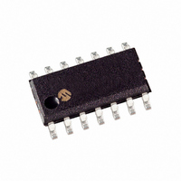
PIC16F630-I/SL Microchip Technology, PIC16F630-I/SL Datasheet - Page 67

PIC16F630-I/SL
Manufacturer Part Number
PIC16F630-I/SL
Description
IC MCU FLASH 1KX14 EEPROM 14SOIC
Manufacturer
Microchip Technology
Series
PIC® 16Fr
Datasheets
1.PIC16F616T-ISL.pdf
(8 pages)
2.PIC12F629T-ISN.pdf
(24 pages)
3.PIC16F630-ISL.pdf
(132 pages)
4.PIC16F630-ISL.pdf
(2 pages)
5.PIC16F630-ISL.pdf
(10 pages)
6.PIC16F676-EP.pdf
(132 pages)
7.PIC16F676-ISL.pdf
(130 pages)
Specifications of PIC16F630-I/SL
Program Memory Type
FLASH
Program Memory Size
1.75KB (1K x 14)
Package / Case
14-SOIC (3.9mm Width), 14-SOL
Core Processor
PIC
Core Size
8-Bit
Speed
20MHz
Peripherals
Brown-out Detect/Reset, POR, WDT
Number Of I /o
12
Eeprom Size
128 x 8
Ram Size
64 x 8
Voltage - Supply (vcc/vdd)
2 V ~ 5.5 V
Oscillator Type
Internal
Operating Temperature
-40°C ~ 85°C
Processor Series
PIC16F
Core
PIC
Data Bus Width
8 bit
Data Ram Size
64 B
Interface Type
RS- 232/USB
Maximum Clock Frequency
20 MHz
Number Of Programmable I/os
12
Number Of Timers
2
Operating Supply Voltage
2 V to 5.5 V
Maximum Operating Temperature
+ 85 C
Mounting Style
SMD/SMT
3rd Party Development Tools
52715-96, 52716-328, 52717-734
Development Tools By Supplier
PG164130, DV164035, DV244005, DV164005, PG164120, ICE2000, DM163014, DM164120-4
Minimum Operating Temperature
- 40 C
Package
14SOIC N
Device Core
PIC
Family Name
PIC16
Maximum Speed
20 MHz
Lead Free Status / RoHS Status
Lead free / RoHS Compliant
Data Converters
-
Connectivity
-
Lead Free Status / Rohs Status
Lead free / RoHS Compliant
Available stocks
Company
Part Number
Manufacturer
Quantity
Price
Company:
Part Number:
PIC16F630-I/SL
Manufacturer:
TriQuint
Quantity:
1 200
Company:
Part Number:
PIC16F630-I/SL
Manufacturer:
MICROCHI
Quantity:
1 743
Part Number:
PIC16F630-I/SL
Manufacturer:
MICROCHIP/微芯
Quantity:
20 000
9.4.1
External interrupt on RA2/INT pin is edge-triggered;
either rising if INTEDG bit (OPTION<6>) is set, or
falling, if INTEDG bit is clear. When a valid edge
appears
(INTCON<1>) is set. This interrupt can be disabled by
clearing the INTE control bit (INTCON<4>). The INTF
bit must be cleared in software in the Interrupt Service
Routine before re-enabling this interrupt. The RA2/INT
interrupt can wake-up the processor from SLEEP if the
INTE bit was set prior to going into SLEEP. The status
of the GIE bit decides whether or not the processor
branches to the interrupt vector following wake-up. See
Section 9.7 for details on SLEEP and Figure 9-13 for
timing of wake-up from SLEEP through RA2/INT
interrupt.
FIGURE 9-11:
© 2007 Microchip Technology Inc.
INSTRUCTION FLOW
Note:
Note 1: INTF flag is sampled here (every Q1).
GIE bit
(INTCON<7>)
INTF Flag
(INTCON<1>)
CLKOUT
INT pin
OSC1
Instruction
Executed
Instruction
Fetched
PC
2: Asynchronous interrupt latency = 3-4 T
3: CLKOUT is available only in RC Oscillator mode.
4: For minimum width of INT pulse, refer to AC specs.
5: INTF is enabled to be set any time during the Q4-Q1 cycles.
on
The ANSEL (91h) and CMCON (19h)
registers must be initialized to configure an
analog channel as a digital input. Pins
configured as analog inputs will read ‘0’.
The ANSEL register is defined for the
PIC16F676.
RA2/INT INTERRUPT
is the same whether Inst (PC) is a single cycle or a 2-cycle instruction.
3
the
Q1
Inst (PC-1)
RA2/INT
Inst (PC)
INT PIN INTERRUPT TIMING
1
Q2
PC
Q3
4
pin,
Q4
5
Q1
the
Inst (PC+1)
Inst (PC)
Q2
1
INTF
PC+1
CY
Q3
. Synchronous latency = 3 T
bit
Q4
Interrupt Latency
Q1
Dummy Cycle
Q2
9.4.2
An overflow (FFh → 00h) in the TMR0 register will
set the T0IF (INTCON<2>) bit. The interrupt can
be
(INTCON<5>) bit. For operation of the Timer0 module,
see Section 4.0.
9.4.3
An input change on PORTA change sets the RAIF
(INTCON<0>) bit. The interrupt can be enabled/
disabled by setting/clearing the RAIE (INTCON<3>)
bit. Plus individual pins can be configured through the
IOCA register.
9.4.4
See Section 6.9 for description of comparator interrupt.
9.4.5
After a conversion is complete, the ADIF flag (PIR<6>)
is set. The interrupt can be enabled/disabled by setting
or clearing ADIE (PIE<6>).
See Section 7.0 for operation of the A/D converter
interrupt.
PC+1
—
Note:
Q3
enabled/disabled
Q4
CY
2
If a change on the I/O pin should occur
when the read operation is being executed
(start of the Q2 cycle), then the RAIF inter-
rupt flag may not get set.
, where T
TMR0 INTERRUPT
PORTA INTERRUPT
COMPARATOR INTERRUPT
A/D CONVERTER INTERRUPT
Q1
Dummy Cycle
PIC16F630/676
Inst (0004h)
Q2
CY
0004h
= instruction cycle time. Latency
Q3
by
Q4
setting/clearing
Q1
DS40039E-page 65
Inst (0005h)
Q2
Inst (0004h)
0005h
Q3
Q4
T0IE


