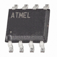
ATTINY13A-SSH Atmel, ATTINY13A-SSH Datasheet - Page 110

ATTINY13A-SSH
Manufacturer Part Number
ATTINY13A-SSH
Description
IC MCU AVR 1K FLASH 20MHZ 8SOIC
Manufacturer
Atmel
Series
AVR® ATtinyr
Specifications of ATTINY13A-SSH
Core Processor
AVR
Core Size
8-Bit
Speed
20MHz
Peripherals
Brown-out Detect/Reset, POR, PWM, WDT
Number Of I /o
6
Program Memory Size
1KB (512 x 16)
Program Memory Type
FLASH
Eeprom Size
64 x 8
Ram Size
64 x 8
Voltage - Supply (vcc/vdd)
1.8 V ~ 5.5 V
Data Converters
A/D 4x10b
Oscillator Type
Internal
Operating Temperature
-40°C ~ 85°C
Package / Case
8-SOIC (3.9mm Width)
Processor Series
ATTINY1x
Core
AVR8
Data Bus Width
8 bit
Data Ram Size
64 B
Interface Type
SPI
Maximum Clock Frequency
20 MHz
Number Of Programmable I/os
6
Number Of Timers
1
Maximum Operating Temperature
+ 85 C
Mounting Style
SMD/SMT
3rd Party Development Tools
EWAVR, EWAVR-BL
Development Tools By Supplier
ATAVRDRAGON, ATSTK500, ATSTK600, ATAVRISP2, ATAVRONEKIT, ATAKSTK511
Minimum Operating Temperature
- 40 C
On-chip Adc
4-ch x 10-bit
For Use With
ATSTK600 - DEV KIT FOR AVR/AVR32770-1007 - ISP 4PORT ATMEL AVR MCU SPI/JTAGATAVRDRAGON - KIT DRAGON 32KB FLASH MEM AVRATAVRISP2 - PROGRAMMER AVR IN SYSTEMATJTAGICE2 - AVR ON-CHIP D-BUG SYSTEM
Lead Free Status / RoHS Status
Lead free / RoHS Compliant
Connectivity
-
Lead Free Status / Rohs Status
Lead free / RoHS Compliant
- Current page: 110 of 176
- Download datasheet (5Mb)
17.7.1
110
ATtiny13A
High-Voltage Serial Programming Algorithm
Table 17-10. Pin Name Mapping
The minimum period for the Serial Clock Input (SCI) during High-voltage Serial Programming is
220 ns.
Table 17-11. Pin Values Used to Enter Programming Mode
To program and verify the ATtiny13A in the High-voltage Serial Programming mode, the follow-
ing sequence is recommended (See instruction formats in
The following algorithm puts the device in High-voltage Serial Programming mode:
If the rise time of the Vcc is unable to fulfill the requirements listed above, the following alterna-
tive algorithm can be used.
Signal Name in High-voltage
Serial Programming Mode
SDI
SII
SDO
SCI
Pin
SDI
SII
SDO
1. Set Prog_enable pins listed in
2. Apply 4.5 - 5.5V between VCC and GND. Ensure that Vcc reaches at least 1.8V within
3. Wait 20 - 60 µs, and apply 11.5 - 12.5V to RESET.
4. Keep the Prog_enable pins unchanged for at least 10µs after the High-voltage has
5. Release the Prog_enable[2] pin to avoid drive contention on the Prog_enable[2]/SDO
6. Wait at least 300µs before giving any serial instructions on SDI/SII.
7. Exit Programming mode by power the device down or by bringing RESET pin to 0V.
1. Set Prog_enable pins listed in
2. Apply 4.5 - 5.5V between VCC and GND.
3. Monitor Vcc, and as soon as Vcc reaches 0.9 - 1.1V, apply 11.5 - 12.5V to RESET.
4. Keep the Prog_enable pins unchanged for at least 10µs after theHigh-voltage has been
5. Release the Prog_enable[2] pin to avoid drive contention on the Prog_enable[2]/SDO
the next 20 µs.
been applied to ensure the Prog_enable Signature has been latched.
pin.
applied to ensure the Prog_enable Signature has been latched.
pin.
Symbol
Prog_enable[0]
Prog_enable[1]
Prog_enable[2]
Pin Name
PB0
PB1
PB2
PB3
Table 17-11
Table 17-11
I/O
I
I
O
I
to “000”, RESET pin to “0” and Vcc to 0V.
to “000”, RESET pin to “0” and Vcc to 0V.
Function
Serial Data Input
Serial Instruction Input
Serial Data Output
Serial Clock Input (min. 220ns period)
Table 17-13 on page
Value
0
0
0
111):
8126E–AVR–07/10
Related parts for ATTINY13A-SSH
Image
Part Number
Description
Manufacturer
Datasheet
Request
R

Part Number:
Description:
IC MCU AVR 1K FLASH 20MHZ 8SOIC
Manufacturer:
Atmel
Datasheet:

Part Number:
Description:
Manufacturer:
Atmel Corporation
Datasheet:

Part Number:
Description:
IC MCU AVR 1K FLASH 20MHZ 8SOIC
Manufacturer:
Atmel
Datasheet:

Part Number:
Description:
IC MCU AVR 1K FLASH 10MHZ 20-MLF
Manufacturer:
Atmel
Datasheet:

Part Number:
Description:
IC MCU AVR 1K FLASH 20MHZ 8DIP
Manufacturer:
Atmel
Datasheet:

Part Number:
Description:
MCU AVR 1KB FLASH 20MHZ 3X3 QFN
Manufacturer:
Atmel
Datasheet:

Part Number:
Description:
IC MCU AVR 1K FLASH 20MHZ 8SOIC
Manufacturer:
Atmel
Datasheet:

Part Number:
Description:
IC MCU AVR 1K 5V 20MHZ 8DIP
Manufacturer:
Atmel
Datasheet:

Part Number:
Description:
IC MCU AVR 1K 5V 20MHZ 8SOIC
Manufacturer:
Atmel
Datasheet:

Part Number:
Description:
IC MCU AVR 1K 5V 20MHZ 8SOIC
Manufacturer:
Atmel
Datasheet:

Part Number:
Description:
IC MCU AVR 1K FLASH 20MHZ 8DIP
Manufacturer:
Atmel
Datasheet:

Part Number:
Description:
IC MCU AVR 1K FLASH 20MHZ 8SOIC
Manufacturer:
Atmel
Datasheet:


