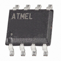
ATTINY13A-SSH Atmel, ATTINY13A-SSH Datasheet - Page 24

ATTINY13A-SSH
Manufacturer Part Number
ATTINY13A-SSH
Description
IC MCU AVR 1K FLASH 20MHZ 8SOIC
Manufacturer
Atmel
Series
AVR® ATtinyr
Specifications of ATTINY13A-SSH
Core Processor
AVR
Core Size
8-Bit
Speed
20MHz
Peripherals
Brown-out Detect/Reset, POR, PWM, WDT
Number Of I /o
6
Program Memory Size
1KB (512 x 16)
Program Memory Type
FLASH
Eeprom Size
64 x 8
Ram Size
64 x 8
Voltage - Supply (vcc/vdd)
1.8 V ~ 5.5 V
Data Converters
A/D 4x10b
Oscillator Type
Internal
Operating Temperature
-40°C ~ 85°C
Package / Case
8-SOIC (3.9mm Width)
Processor Series
ATTINY1x
Core
AVR8
Data Bus Width
8 bit
Data Ram Size
64 B
Interface Type
SPI
Maximum Clock Frequency
20 MHz
Number Of Programmable I/os
6
Number Of Timers
1
Maximum Operating Temperature
+ 85 C
Mounting Style
SMD/SMT
3rd Party Development Tools
EWAVR, EWAVR-BL
Development Tools By Supplier
ATAVRDRAGON, ATSTK500, ATSTK600, ATAVRISP2, ATAVRONEKIT, ATAKSTK511
Minimum Operating Temperature
- 40 C
On-chip Adc
4-ch x 10-bit
For Use With
ATSTK600 - DEV KIT FOR AVR/AVR32770-1007 - ISP 4PORT ATMEL AVR MCU SPI/JTAGATAVRDRAGON - KIT DRAGON 32KB FLASH MEM AVRATAVRISP2 - PROGRAMMER AVR IN SYSTEMATJTAGICE2 - AVR ON-CHIP D-BUG SYSTEM
Lead Free Status / RoHS Status
Lead free / RoHS Compliant
Connectivity
-
Lead Free Status / Rohs Status
Lead free / RoHS Compliant
- Current page: 24 of 176
- Download datasheet (5Mb)
6.1.4
6.2
6.2.1
24
Clock Sources
ATtiny13A
ADC Clock – clk
External Clock
The ADC is provided with a dedicated clock domain. This allows halting the CPU and I/O clocks
in order to reduce noise generated by digital circuitry. This gives more accurate ADC conversion
results.
The device has the following clock source options, selectable by Flash fuse bits as shown
below. The clock from the selected source is input to the AVR clock generator, and routed to the
appropriate modules.
Table 6-1.
Note:
The various choices for each clocking option is given in the following sections. When the CPU
wakes up from Power-down or Power-save, the selected clock source is used to time the start-
up, ensuring stable Oscillator operation before instruction execution starts. When the CPU starts
from reset, there is an additional delay allowing the power to reach a stable level before com-
mencing normal operation. The Watchdog Oscillator is used for timing this real-time part of the
start-up time. The number of WDT Oscillator cycles used for each time-out is shown in
2.
Table 6-2.
To drive the device from an external clock source, CLKI should be driven as shown in
2. To run the device on an external clock, the CKSEL fuses must be programmed to “00”.
Figure 6-2.
Device Clocking Option
External Clock (see
Calibrated Internal 4.8/9.6 MHz Oscillator (see
Internal 128 kHz Oscillator (see
ADC
1. For all fuses “1” means unprogrammed while “0” means programmed.
Typ Time-out
Device Clocking Options Select
Number of Watchdog Oscillator Cycles
External Clock Drive Configuration
EXTERNAL
64 ms
4 ms
page
SIGNAL
CLOCK
24)
page
26)
page
25)
CLKI
GND
Number of Cycles
8K (8,192)
512
CKSEL[1:0]
01, 10
00
11
(1)
8126E–AVR–07/10
Figure 6-
Table 6-
Related parts for ATTINY13A-SSH
Image
Part Number
Description
Manufacturer
Datasheet
Request
R

Part Number:
Description:
IC MCU AVR 1K FLASH 20MHZ 8SOIC
Manufacturer:
Atmel
Datasheet:

Part Number:
Description:
Manufacturer:
Atmel Corporation
Datasheet:

Part Number:
Description:
IC MCU AVR 1K FLASH 20MHZ 8SOIC
Manufacturer:
Atmel
Datasheet:

Part Number:
Description:
IC MCU AVR 1K FLASH 10MHZ 20-MLF
Manufacturer:
Atmel
Datasheet:

Part Number:
Description:
IC MCU AVR 1K FLASH 20MHZ 8DIP
Manufacturer:
Atmel
Datasheet:

Part Number:
Description:
MCU AVR 1KB FLASH 20MHZ 3X3 QFN
Manufacturer:
Atmel
Datasheet:

Part Number:
Description:
IC MCU AVR 1K FLASH 20MHZ 8SOIC
Manufacturer:
Atmel
Datasheet:

Part Number:
Description:
IC MCU AVR 1K 5V 20MHZ 8DIP
Manufacturer:
Atmel
Datasheet:

Part Number:
Description:
IC MCU AVR 1K 5V 20MHZ 8SOIC
Manufacturer:
Atmel
Datasheet:

Part Number:
Description:
IC MCU AVR 1K 5V 20MHZ 8SOIC
Manufacturer:
Atmel
Datasheet:

Part Number:
Description:
IC MCU AVR 1K FLASH 20MHZ 8DIP
Manufacturer:
Atmel
Datasheet:

Part Number:
Description:
IC MCU AVR 1K FLASH 20MHZ 8SOIC
Manufacturer:
Atmel
Datasheet:


