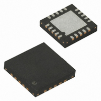
ATTINY45V-10MU Atmel, ATTINY45V-10MU Datasheet - Page 115

ATTINY45V-10MU
Manufacturer Part Number
ATTINY45V-10MU
Description
IC AVR MCU FLASH 4K 10MHZ 20MLF
Manufacturer
Atmel
Series
AVR® ATtinyr
Specifications of ATTINY45V-10MU
Core Processor
AVR
Core Size
8-Bit
Speed
10MHz
Connectivity
USI
Peripherals
Brown-out Detect/Reset, POR, PWM, WDT
Number Of I /o
6
Program Memory Size
4KB (2K x 16)
Program Memory Type
FLASH
Eeprom Size
256 x 8
Ram Size
256 x 8
Voltage - Supply (vcc/vdd)
1.8 V ~ 5.5 V
Data Converters
A/D 4x10b
Oscillator Type
Internal
Operating Temperature
-40°C ~ 85°C
Package / Case
20-MLF®, QFN
Processor Series
ATTINY4x
Core
AVR8
Data Bus Width
8 bit
Data Ram Size
256 B
Interface Type
USI
Maximum Clock Frequency
10 MHz
Number Of Programmable I/os
6
Number Of Timers
2
Operating Supply Voltage
1.8 V to 5.5 V
Maximum Operating Temperature
+ 85 C
Mounting Style
SMD/SMT
Minimum Operating Temperature
- 40 C
On-chip Adc
10 bit, 4 Channel
Package
20MLF EP
Device Core
AVR
Family Name
ATtiny
Maximum Speed
10 MHz
For Use With
ATSTK600-DIP40 - STK600 SOCKET/ADAPTER 40-PDIPATAVRBC100 - REF DESIGN KIT BATTERY CHARGER770-1007 - ISP 4PORT ATMEL AVR MCU SPI/JTAGATAVRDRAGON - KIT DRAGON 32KB FLASH MEM AVRATAVRISP2 - PROGRAMMER AVR IN SYSTEMATJTAGICE2 - AVR ON-CHIP D-BUG SYSTEM
Lead Free Status / RoHS Status
Lead free / RoHS Compliant
Available stocks
Company
Part Number
Manufacturer
Quantity
Price
Part Number:
ATTINY45V-10MU
Manufacturer:
ATMEL/爱特梅尔
Quantity:
20 000
- Current page: 115 of 236
- Download datasheet (5Mb)
15.3.4
2586M–AVR–07/10
Two-wire Mode
The code is size optimized using only eight instructions (plus return). The code example
assumes that the DO and USCK pins have been enabled as outputs in DDRB. The value stored
in register r16 prior to the function is called is transferred to the master device, and when the
transfer is completed the data received from the master is stored back into the register r16.
Note that the first two instructions is for initialization, only, and need only be executed once.
These instructions set three-wire mode and positive edge clock. The loop is repeated until the
USI Counter Overflow Flag is set.
The USI two-wire mode is compliant to the Inter IC (TWI) bus protocol, but without slew rate lim-
iting on outputs and without input noise filtering. Pin names used in this mode are SCL and SDA.
Figure 15-4. Two-wire Mode Operation, Simplified Diagram
...
SlaveSPITransfer:
SlaveSPITransfer_loop:
out
ldi
out
in
sbrs
rjmp
in
ret
SLAVE
MASTER
USISR,r16
Bit7
Bit7
USIDR,r16
r16,(1<<USIOIF)
r16, USISR
r16, USIOIF
SlaveSPITransfer_loop
r16,USIDR
Bit6
Bit6
Bit5
Bit5
Bit4
Bit4
Bit3
Bit3
Bit2
Bit2
Bit1
Bit1
Bit0
Bit0
Two-wire Clock
Control Unit
PORTxn
HOLD
SCL
SDA
SCL
SDA
SCL
VCC
115
Related parts for ATTINY45V-10MU
Image
Part Number
Description
Manufacturer
Datasheet
Request
R

Part Number:
Description:
IC AVR MCU 4K 10MHZ 8SOIC
Manufacturer:
Atmel
Datasheet:

Part Number:
Description:
MCU AVR 4KB FLASH 10MHZ 8SOIC
Manufacturer:
Atmel
Datasheet:

Part Number:
Description:
IC MCU AVR 4K FLASH 10MHZ 8TSSOP
Manufacturer:
Atmel
Datasheet:

Part Number:
Description:
IC AVR MCU 4K 10MHZ 8DIP
Manufacturer:
Atmel
Datasheet:

Part Number:
Description:
MCU AVR 4KB FLASH 10MHZ 8TSSOP
Manufacturer:
Atmel
Datasheet:

Part Number:
Description:
IC MCU AVR 4KB FLASH 20MHZ 8SOIC
Manufacturer:
Atmel
Datasheet:

Part Number:
Description:
MCU AVR 4KB FLASH 10MHZ 20QFN
Manufacturer:
Atmel
Datasheet:

Part Number:
Description:
IC AVR MCU 4K 10MHZ 8DIP
Manufacturer:
Atmel
Datasheet:

Part Number:
Description:
IC AVR MCU 4K 10MHZ 8SOIC
Manufacturer:
Atmel
Datasheet:

Part Number:
Description:
8-bit Microcontrollers - MCU 4K FL, 256B EESRAM, ADC,8 PINS - 10MHz
Manufacturer:
Atmel

Part Number:
Description:
Manufacturer:
Atmel Corporation
Datasheet:

Part Number:
Description:
Manufacturer:
Atmel Corporation
Datasheet:

Part Number:
Description:
IC AVR MCU 4K 20MHZ 8SOIC
Manufacturer:
Atmel
Datasheet:


