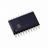
DSPIC33FJ12MC201-I/SO Microchip Technology, DSPIC33FJ12MC201-I/SO Datasheet - Page 216

DSPIC33FJ12MC201-I/SO
Manufacturer Part Number
DSPIC33FJ12MC201-I/SO
Description
IC DSPIC MCU/DSP 12K 20SOIC
Manufacturer
Microchip Technology
Series
dsPIC™ 33Fr
Datasheets
1.PIC24HJ12GP201-ISO.pdf
(84 pages)
2.DSPIC33FJ12MC201-ISO.pdf
(288 pages)
3.DSPIC33FJ12MC201-ISO.pdf
(14 pages)
4.DSPIC33FJ12MC201-IP.pdf
(284 pages)
Specifications of DSPIC33FJ12MC201-I/SO
Program Memory Type
FLASH
Program Memory Size
12KB (12K x 8)
Package / Case
20-SOIC (7.5mm Width)
Core Processor
dsPIC
Core Size
16-Bit
Speed
40 MIPs
Connectivity
I²C, IrDA, SPI, UART/USART
Peripherals
Brown-out Detect/Reset, Motor Control PWM, QEI, POR, PWM, WDT
Number Of I /o
15
Ram Size
1K x 8
Voltage - Supply (vcc/vdd)
3 V ~ 3.6 V
Data Converters
A/D 4x10b
Oscillator Type
Internal
Operating Temperature
-40°C ~ 85°C
Product
DSCs
Data Bus Width
16 bit
Processor Series
DSPIC33F
Core
dsPIC
Maximum Clock Frequency
40 MHz
Number Of Programmable I/os
15
Data Ram Size
1 KB
Maximum Operating Temperature
+ 85 C
Mounting Style
SMD/SMT
3rd Party Development Tools
52713-733, 52714-737, 53276-922, EWDSPIC
Development Tools By Supplier
PG164130, DV164035, DV244005, DV164005, PG164120, DM240001, DV164033
Minimum Operating Temperature
- 40 C
Lead Free Status / RoHS Status
Lead free / RoHS Compliant
For Use With
DV164033 - KIT START EXPLORER 16 MPLAB ICD2DM240001 - BOARD DEMO PIC24/DSPIC33/PIC32
Eeprom Size
-
Lead Free Status / Rohs Status
Lead free / RoHS Compliant
- PIC24HJ12GP201-ISO PDF datasheet
- DSPIC33FJ12MC201-ISO PDF datasheet #2
- DSPIC33FJ12MC201-ISO PDF datasheet #3
- DSPIC33FJ12MC201-IP PDF datasheet #4
- Current page: 216 of 284
- Download datasheet (5Mb)
dsPIC33FJ12MC201/202
20.2
All of the dsPIC33FJ12MC201/202 devices power their
core digital logic at a nominal 2.5V. This can create a
conflict for designs that are required to operate at a
higher typical voltage, such as 3.3V. To simplify system
design, all devices in the dsPIC33FJ12MC201/202
family incorporate an on-chip regulator that allows the
device to run its core logic from V
The regulator provides power to the core from the other
V
(less than 5 ohms) capacitor (such as tantalum or
ceramic) must be connected to the V
(Figure 20-1). This helps to maintain the stability of the
regulator. The recommended value for the filter capac-
itor is provided in Table 23-13 located in Section 23.1
“DC Characteristics”.
On a POR
voltage regulator to generate an output voltage. During
this time, designated as T
disabled. T
resumes operation after any power-down.
FIGURE 20-1:
DS70265B-page 214
DD
Note 1:
pins. When the regulator is enabled, a low-ESR
On-Chip Voltage Regulator
,
STARTUP
it takes approximately 20 μs for the on-chip
C
F
These are typical operating voltages. Refer
to Section TABLE 23-13: “Internal Volt-
age Regulator Specifications” located in
Section 23.1 “DC Characteristics” for the
full operating ranges of V
3.3V
is applied every time the device
CONNECTIONS FOR THE
ON-CHIP VOLTAGE
REGULATOR
V
V
V
DD
DDCORE
SS
dsPIC33F
STARTUP
/V
DD
CAP
, code execution is
DD
.
DDCORE
and V
(1)
DDCORE
/V
CAP
.
Preliminary
pin
20.3
The Brown-out Reset (BOR) module is based on an
internal voltage reference circuit that monitors the reg-
ulated supply voltage V
the BOR module is to generate a device Reset when a
brown-out condition occurs. Brown-out conditions are
generally caused by glitches on the AC mains (for
example, missing portions of the AC cycle waveform
due to bad power transmission lines, or voltage sags
due to excessive current draw when a large inductive
load is turned on).
A BOR generates a Reset pulse, which resets the
device. The BOR selects the clock source, based on
the device Configuration bit values (FNOSC<2:0> and
POSCMD<1:0>).
If an oscillator mode is selected, the BOR activates the
Oscillator Start-up Timer (OST). The system clock is
held until OST expires. If the PLL is used, the clock is
held until the LOCK bit (OSCCON<5>) is ‘1’.
Concurrently, the PWRT time-out (TPWRT) is applied
before the internal Reset is released. If TPWRT = 0 and
a crystal oscillator is being used, then a nominal delay
of TFSCM = 100 is applied. The total delay in this case
is TFSCM.
The BOR Status bit (RCON<1>) is set to indicate that
a BOR has occurred. The BOR circuit, if enabled, con-
tinues to operate while in Sleep or Idle modes and
resets the device should VDD fall below the BOR
threshold voltage.
BOR: Brown-Out Reset
DDCORE
© 2007 Microchip Technology Inc.
. The main purpose of
Related parts for DSPIC33FJ12MC201-I/SO
Image
Part Number
Description
Manufacturer
Datasheet
Request
R

Part Number:
Description:
IC, DSC, 16BIT, 12KB, 40MHZ, 3.6V, DIP28
Manufacturer:
Microchip Technology
Datasheet:

Part Number:
Description:
Manufacturer:
Microchip Technology Inc.
Datasheet:

Part Number:
Description:
Manufacturer:
Microchip Technology Inc.
Datasheet:

Part Number:
Description:
Manufacturer:
Microchip Technology Inc.
Datasheet:

Part Number:
Description:
Manufacturer:
Microchip Technology Inc.
Datasheet:

Part Number:
Description:
Manufacturer:
Microchip Technology Inc.
Datasheet:

Part Number:
Description:
Manufacturer:
Microchip Technology Inc.
Datasheet:

Part Number:
Description:
Manufacturer:
Microchip Technology Inc.
Datasheet:

Part Number:
Description:
Manufacturer:
Microchip Technology Inc.
Datasheet:


