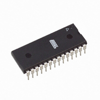
ATMEGA168-20PU Atmel, ATMEGA168-20PU Datasheet - Page 297

ATMEGA168-20PU
Manufacturer Part Number
ATMEGA168-20PU
Description
IC AVR MCU 16K 20MHZ 28DIP
Manufacturer
Atmel
Series
AVR® ATmegar
Datasheets
1.ATAVRTS2080B.pdf
(378 pages)
2.ATMEGA48-20AU.pdf
(35 pages)
3.ATMEGA88-20MU.pdf
(33 pages)
4.ATMEGA168-20AU.pdf
(359 pages)
Specifications of ATMEGA168-20PU
Core Processor
AVR
Core Size
8-Bit
Speed
20MHz
Connectivity
I²C, SPI, UART/USART
Peripherals
Brown-out Detect/Reset, POR, PWM, WDT
Number Of I /o
23
Program Memory Size
16KB (8K x 16)
Program Memory Type
FLASH
Eeprom Size
512 x 8
Ram Size
1K x 8
Voltage - Supply (vcc/vdd)
2.7 V ~ 5.5 V
Data Converters
A/D 6x10b
Oscillator Type
Internal
Operating Temperature
-40°C ~ 85°C
Package / Case
28-DIP (0.300", 7.62mm)
Processor Series
ATMEGA16x
Core
AVR8
Data Bus Width
8 bit
Data Ram Size
1 KB
Interface Type
2-Wire, SPI, USART, Serial
Maximum Clock Frequency
20 MHz
Number Of Programmable I/os
23
Number Of Timers
3
Operating Supply Voltage
2.7 V to 5.5 V
Maximum Operating Temperature
+ 85 C
Mounting Style
Through Hole
3rd Party Development Tools
EWAVR, EWAVR-BL
Development Tools By Supplier
ATAVRDRAGON, ATSTK500, ATSTK600, ATAVRISP2, ATAVRONEKIT
Minimum Operating Temperature
- 40 C
On-chip Adc
10 bit, 6 Channel
A/d Inputs
6-Channel, 10-Bit
Cpu Speed
20 MIPS
Eeprom Memory
512 Bytes
Input Output
23
Interface
I2C/SPI/UART/USART
Memory Type
Flash
Number Of Bits
8
Package Type
28-pin PDIP
Programmable Memory
16K Bytes
Timers
2-8-bit, 1-16-bit
Voltage, Range
4.5-5.5 V
Controller Family/series
AVR MEGA
No. Of I/o's
23
Eeprom Memory Size
512Byte
Ram Memory Size
1KB
Rohs Compliant
Yes
For Use With
ATSTK600-TQFP32 - STK600 SOCKET/ADAPTER 32-TQFPATSTK600 - DEV KIT FOR AVR/AVR32770-1007 - ISP 4PORT ATMEL AVR MCU SPI/JTAGATAVRDRAGON - KIT DRAGON 32KB FLASH MEM AVRATAVRISP2 - PROGRAMMER AVR IN SYSTEMATJTAGICE2 - AVR ON-CHIP D-BUG SYSTEM
Lead Free Status / RoHS Status
Lead free / RoHS Compliant
Available stocks
Company
Part Number
Manufacturer
Quantity
Price
Part Number:
ATMEGA168-20PU
Manufacturer:
ATMEL/爱特梅尔
Quantity:
20 000
- ATAVRTS2080B PDF datasheet
- ATMEGA48-20AU PDF datasheet #2
- ATMEGA88-20MU PDF datasheet #3
- ATMEGA168-20AU PDF datasheet #4
- Current page: 297 of 359
- Download datasheet (3Mb)
Table 25-17. Serial Programming Instruction Set
2545E–AVR–02/05
Instruction
Programming Enable
Chip Erase
Read Program Memory
Load Program Memory Page
Write Program Memory Page
Read EEPROM Memory
Write EEPROM Memory
6. Any memory location can be verified by using the Read instruction which returns the con-
7. At the end of the programming session, RESET can be set high to commence normal
8. Power-off sequence (if needed):
Table 25-16. Typical Wait Delay Before Writing the Next Flash or EEPROM Location
Figure 25-11. Serial Programming Waveforms
Symbol
t
t
t
WD_FLASH
WD_EEPROM
WD_ERASE
tent at the selected address at serial output MISO.
operation.
Set RESET to “1”.
Turn V
1010 1100
1010 1100
0010 H000
0100 H000
0100 1100
1010 0000
1100 0000
SERIAL DATA OUTPUT
SERIAL CLOCK INPUT
Byte 1
SERIAL DATA INPUT
CC
power off.
SAMPLE
0101 0011
100x xxxx
000a aaaa
000x xxxx
000a aaaa
000x xxaa
000x xxaa
(MOSI)
(MISO)
(SCK)
Byte 2
Instruction Format
MSB
MSB
xxxx xxxx
xxxx xxxx
bbbb bbbb
xxbb bbbb
bbxx xxxx
bbbb bbbb
bbbb bbbb
Byte 3
xxxx xxxx
xxxx xxxx
oooo oooo
iiii iiii
xxxx xxxx
oooo oooo
iiii iiii
Byte4
Operation
Enable Serial Programming after
RESET goes low.
Chip Erase EEPROM and Flash.
Read H (high or low) data o from
Program memory at word address a:b.
Write H (high or low) data i to Program
Memory page at word address b. Data
low byte must be loaded before Data
high byte is applied within the same
address.
Write Program Memory Page at
address a:b.
Read data o from EEPROM memory at
address a:b.
Write data i to EEPROM memory at
address a:b.
ATmega48/88/168
Minimum Wait Delay
4.5 ms
3.6 ms
9.0 ms
LSB
LSB
297
Related parts for ATMEGA168-20PU
Image
Part Number
Description
Manufacturer
Datasheet
Request
R

Part Number:
Description:
Manufacturer:
Atmel Corporation
Datasheet:

Part Number:
Description:
Manufacturer:
Atmel Corporation
Datasheet:

Part Number:
Description:
Manufacturer:
ATMEL Corporation
Datasheet:

Part Number:
Description:
IC AVR MCU 16K 20MHZ 32TQFP
Manufacturer:
Atmel
Datasheet:

Part Number:
Description:
IC AVR MCU 16K 20MHZ 32-QFN
Manufacturer:
Atmel
Datasheet:

Part Number:
Description:
MCU AVR 16K FLASH 15MHZ 32-TQFP
Manufacturer:
Atmel
Datasheet:

Part Number:
Description:
MCU AVR 16K FLASH 15MHZ 32-QFN
Manufacturer:
Atmel
Datasheet:

Part Number:
Description:
IC AVR MCU 16K 20MHZ 32TQFP
Manufacturer:
Atmel
Datasheet:

Part Number:
Description:
MCU AVR 16KB FLASH 20MHZ 32QFN
Manufacturer:
Atmel
Datasheet:

Part Number:
Description:
MCU AVR 16KB FLASH 20MHZ 32TQFP
Manufacturer:
Atmel
Datasheet:

Part Number:
Description:
IC MCU AVR 16K FLASH 32-QFN
Manufacturer:
Atmel
Datasheet:


