AT89C5115-RATUM Atmel, AT89C5115-RATUM Datasheet - Page 83
AT89C5115-RATUM
Manufacturer Part Number
AT89C5115-RATUM
Description
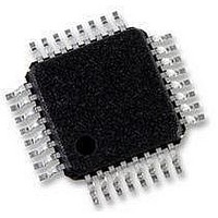
IC 8051 MCU FLASH 16K 32VQFP
Manufacturer
Atmel
Series
89Cr
Datasheet
1.T89C5115-RATIM.pdf
(113 pages)
Specifications of AT89C5115-RATUM
Core Processor
8051
Core Size
8-Bit
Speed
40MHz
Connectivity
UART/USART
Peripherals
POR, PWM, WDT
Number Of I /o
20
Program Memory Size
16KB (16K x 8)
Program Memory Type
FLASH
Eeprom Size
2K x 8
Ram Size
512 x 8
Voltage - Supply (vcc/vdd)
3 V ~ 5.5 V
Data Converters
A/D 8x10b
Oscillator Type
External
Operating Temperature
-40°C ~ 85°C
Package / Case
32-TQFP, 32-VQFP
Processor Series
AT89x
Core
8051
Data Bus Width
8 bit
Data Ram Size
512 B
Interface Type
UART
Maximum Clock Frequency
40 MHz
Number Of Programmable I/os
20
Number Of Timers
2
Operating Supply Voltage
3 V to 5.5 V
Maximum Operating Temperature
+ 85 C
Mounting Style
SMD/SMT
3rd Party Development Tools
PK51, CA51, A51, ULINK2
Development Tools By Supplier
CANADAPT28
Minimum Operating Temperature
- 40 C
On-chip Adc
10 bit, 8 Channel
Package
32VQFP
Device Core
8051
Family Name
89C
Maximum Speed
40 MHz
For Use With
AT89OCD-01 - USB EMULATOR FOR AT8XC51 MCU
Lead Free Status / RoHS Status
Lead free / RoHS Compliant
Available stocks
Company
Part Number
Manufacturer
Quantity
Price


Analog-to-Digital
Converter (ADC)
Features
ADC Port1 I/O Functions
VAREF
4128G–8051–02/08
This section describes the on-chip 10-bit analog-to-digital converter of the T89C5115.
Eight ADC channels are available for sampling of the external sources AN0 to AN7. An
analog multiplexer allows the single ADC converter to select one from the 8 ADC chan-
nels as ADC input voltage (ADCIN). ADCIN is converted by the 10-bit-cascaded
potentiometric ADC.
Two modes of conversion are available:
- Standard conversion (8 bits).
- Precision conversion (10 bits).
For the precision conversion, set bit PSIDLE in ADCON register and start conversion.
The device is in a pseudo-idle mode, the CPU does not run but the peripherals are
always running. This mode allows digital noise to be as low as possible, to ensure high
precision conversion.
For this mode it is necessary to work with end of conversion interrupt, which is the only
way to wake the device up.
If another interrupt occurs during the precision conversion, it will be served only after
this conversion is completed.
•
•
•
•
•
•
•
•
•
•
Port 1 pins are general I/O that are shared with the ADC channels. The channel select
bit in ADCF register define which ADC channel/port1 pin will be used as ADCIN. The
remaining ADC channels/port1 pins can be used as general purpose I/O or as the alter-
nate function that is available.
A conversion launched on a channel which are not selected on ADCF register will not
have any effect.
VAREF should be connected to a low impedance point and must remain in the range
specified VAREF absolute maximum range (See section “AC-DC”).
. If the ADC is not used, it is recommended to tie VAREF to VAGND.
8 channels with multiplexed inputs
10-bit cascaded potentiometric ADC
Conversion time 16 micro-seconds (typ.)
Zero Error (offset) ± 2 LSB max
Positive External Reference Voltage Range (VAREF) 2.4 to 3.0-volt (typ.)
ADCIN Range 0 to 3-volt
Integral non-linearity typical 1 LSB, max. 2 LSB
Differential non-linearity typical 0.5 LSB, max. 1 LSB
Conversion Complete Flag or Conversion Complete Interrupt
Selectable ADC Clock
83
Related parts for AT89C5115-RATUM
Image
Part Number
Description
Manufacturer
Datasheet
Request
R

Part Number:
Description:
Manufacturer:
Atmel Corporation
Datasheet:

Part Number:
Description:
IC 8051 MCU FLASH 16K 28SOIC
Manufacturer:
Atmel
Datasheet:

Part Number:
Description:
IC 8051 MCU FLASH 16K 28PLCC
Manufacturer:
Atmel
Datasheet:

Part Number:
Description:
DEV KIT FOR AVR/AVR32
Manufacturer:
Atmel
Datasheet:
Part Number:
Description:
INTERVAL AND WIPE/WASH WIPER CONTROL IC WITH DELAY
Manufacturer:
ATMEL Corporation
Datasheet:
Part Number:
Description:
Low-Voltage Voice-Switched IC for Hands-Free Operation
Manufacturer:
ATMEL Corporation
Datasheet:
Part Number:
Description:
MONOLITHIC INTEGRATED FEATUREPHONE CIRCUIT
Manufacturer:
ATMEL Corporation
Datasheet:
Part Number:
Description:
AM-FM Receiver IC U4255BM-M
Manufacturer:
ATMEL Corporation
Datasheet:
Part Number:
Description:
Monolithic Integrated Feature Phone Circuit
Manufacturer:
ATMEL Corporation
Datasheet:
Part Number:
Description:
Multistandard Video-IF and Quasi Parallel Sound Processing
Manufacturer:
ATMEL Corporation
Datasheet:
Part Number:
Description:
High-performance EE PLD
Manufacturer:
ATMEL Corporation
Datasheet:
Part Number:
Description:
8-bit Flash Microcontroller
Manufacturer:
ATMEL Corporation
Datasheet: