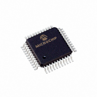
PIC16LF874-04I/PQ Microchip Technology, PIC16LF874-04I/PQ Datasheet - Page 38

PIC16LF874-04I/PQ
Manufacturer Part Number
PIC16LF874-04I/PQ
Description
IC PIC MCU FLASH 4KX14 44MQFP
Manufacturer
Microchip Technology
Series
PIC® 16Fr
Datasheet
1.PIC16F873-04SO.pdf
(218 pages)
Specifications of PIC16LF874-04I/PQ
Core Processor
PIC
Core Size
8-Bit
Speed
4MHz
Connectivity
I²C, SPI, UART/USART
Peripherals
Brown-out Detect/Reset, POR, PWM, WDT
Number Of I /o
33
Program Memory Size
7KB (4K x 14)
Program Memory Type
FLASH
Eeprom Size
128 x 8
Ram Size
192 x 8
Voltage - Supply (vcc/vdd)
2 V ~ 5.5 V
Data Converters
A/D 8x10b
Oscillator Type
External
Operating Temperature
-40°C ~ 85°C
Package / Case
44-MQFP, 44-PQFP
Lead Free Status / RoHS Status
Lead free / RoHS Compliant
Available stocks
Company
Part Number
Manufacturer
Quantity
Price
Company:
Part Number:
PIC16LF874-04I/PQ
Manufacturer:
Microchip Technology
Quantity:
10 000
Part Number:
PIC16LF874-04I/PQ
Manufacturer:
MICROCHIP/微芯
Quantity:
20 000
- Current page: 38 of 218
- Download datasheet (4Mb)
PIC16F87X
3.5
PORTE and TRISE are not implemented on the
PIC16F873 or PIC16F876.
PORTE has three pins (RE0/RD/AN5, RE1/WR/AN6,
and RE2/CS/AN7) which are individually configureable
as inputs or outputs. These pins have Schmitt Trigger
input buffers.
The PORTE pins become the I/O control inputs for the
microprocessor port when bit PSPMODE (TRISE<4>) is
set. In this mode, the user must make certain that the
TRISE<2:0> bits are set, and that the pins are configured
as digital inputs. Also ensure that ADCON1 is configured
for digital I/O. In this mode, the input buffers are TTL.
Register 3-1 shows the TRISE register, which also con-
trols the parallel slave port operation.
PORTE pins are multiplexed with analog inputs. When
selected for analog input, these pins will read as ’0’s.
TRISE controls the direction of the RE pins, even when
they are being used as analog inputs. The user must
make sure to keep the pins configured as inputs when
using them as analog inputs.
TABLE 3-9:
TABLE 3-10:
DS30292C-page 36
RE0/RD/AN5
RE1/WR/AN6
RE2/CS/AN7
Legend: ST = Schmitt Trigger input, TTL = TTL input
Note 1: Input buffers are Schmitt Triggers when in I/O mode and TTL buffers when in Parallel Slave Port mode.
09h
89h
9Fh
Legend: x = unknown, u = unchanged, - = unimplemented, read as ’0’. Shaded cells are not used by PORTE.
Address
Note:
Name
PORTE and TRISE Register
On a Power-on Reset, these pins are con-
figured as analog inputs, and read as ‘0’.
PORTE
TRISE
ADCON1
Name
Bit#
bit0
bit1
bit2
PORTE FUNCTIONS
SUMMARY OF REGISTERS ASSOCIATED WITH PORTE
ADFM
Bit 7
IBF
—
Buffer Type
ST/TTL
ST/TTL
ST/TTL
Bit 6
OBF
—
—
(1)
(1)
(1)
IBOV
Bit 5
I/O port pin or read control input in Parallel Slave Port mode or analog input:
RD
1 = Idle
0 = Read operation. Contents of PORTD register are output to PORTD
I/O port pin or write control input in Parallel Slave Port mode or analog input:
WR
1 = Idle
0 = Write operation. Value of PORTD I/O pins is latched into PORTD
I/O port pin or chip select control input in Parallel Slave Port mode or analog input:
CS
1 = Device is not selected
0 = Device is selected
—
—
register (if chip selected)
I/O pins (if chip selected)
PSPMODE
Bit 4
—
—
PCFG3
Bit 3
—
—
FIGURE 3-8:
PORTE Data Direction Bits
PCFG2
WR
TRIS
Data
Bus
RD
TRIS
WR
Port
Note 1: I/O pins have protection diodes to V
RD Port
Bit 2
RE2
Function
PCFG1
Bit 1
RE1
TRIS Latch
Data Latch
D
D
CK
CK
Q
Q
PCFG0 --0- 0000 --0- 0000
Bit 0
RE0
PORTE BLOCK DIAGRAM
(IN I/O PORT MODE)
2001 Microchip Technology Inc.
Q
---- -xxx ---- -uuu
0000 -111 0000 -111
POR, BOR
Value on:
EN
EN
Schmitt
Trigger
Input
Buffer
D
DD
and V
Value on
RESETS
all other
I/O pin
SS
.
(1)
Related parts for PIC16LF874-04I/PQ
Image
Part Number
Description
Manufacturer
Datasheet
Request
R

Part Number:
Description:
IC MCU FLASH 4KX14 EE A/D 44PLCC
Manufacturer:
Microchip Technology
Datasheet:

Part Number:
Description:
IC PIC MCU FLASH 4KX14 44TQFP
Manufacturer:
Microchip Technology
Datasheet:

Part Number:
Description:
IC MCU FLASH 4KX14 EE A/D 40DIP
Manufacturer:
Microchip Technology
Datasheet:

Part Number:
Description:
IC PIC MCU FLASH 4KX14 44TQFP
Manufacturer:
Microchip Technology
Datasheet:

Part Number:
Description:
IC MCU FLASH 4KX14 EE A/D 44PLCC
Manufacturer:
Microchip Technology
Datasheet:

Part Number:
Description:
IC PIC MCU FLASH 4KX14 44MQFP
Manufacturer:
Microchip Technology
Datasheet:

Part Number:
Description:
IC MCU FLASH 4KX14 EE A/D 40DIP
Manufacturer:
Microchip Technology
Datasheet:

Part Number:
Description:
IC MCU FLASH 4KX14 EEPROM 18SOIC
Manufacturer:
Microchip Technology
Datasheet:

Part Number:
Description:
IC MCU FLASH 4KX14 EEPROM 18DIP
Manufacturer:
Microchip Technology
Datasheet:

Part Number:
Description:
IC MCU FLASH 4KX14 EEPROM 20SSOP
Manufacturer:
Microchip Technology
Datasheet:

Part Number:
Description:
(PIC16LF87 / PIC16LF88) 18/20/28-Pin Enhanced FLASH Microcontrollers with nanoWatt Technology
Manufacturer:
Microchip Technology

Part Number:
Description:
IC MCU FLASH 4KX14 EEPROM 28QFN
Manufacturer:
Microchip Technology
Datasheet:

Part Number:
Description:
IC, 8BIT MCU, PIC16LF, 32MHZ, QFN-28
Manufacturer:
Microchip Technology
Datasheet:

Part Number:
Description:
IC, 8BIT MCU, PIC16LF, 32MHZ, QFN-28
Manufacturer:
Microchip Technology
Datasheet:

Part Number:
Description:
IC, 8BIT MCU, PIC16LF, 32MHZ, DIP-18
Manufacturer:
Microchip Technology
Datasheet:


