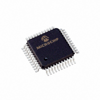
PIC16LF874-04I/PQ Microchip Technology, PIC16LF874-04I/PQ Datasheet - Page 77

PIC16LF874-04I/PQ
Manufacturer Part Number
PIC16LF874-04I/PQ
Description
IC PIC MCU FLASH 4KX14 44MQFP
Manufacturer
Microchip Technology
Series
PIC® 16Fr
Datasheet
1.PIC16F873-04SO.pdf
(218 pages)
Specifications of PIC16LF874-04I/PQ
Core Processor
PIC
Core Size
8-Bit
Speed
4MHz
Connectivity
I²C, SPI, UART/USART
Peripherals
Brown-out Detect/Reset, POR, PWM, WDT
Number Of I /o
33
Program Memory Size
7KB (4K x 14)
Program Memory Type
FLASH
Eeprom Size
128 x 8
Ram Size
192 x 8
Voltage - Supply (vcc/vdd)
2 V ~ 5.5 V
Data Converters
A/D 8x10b
Oscillator Type
External
Operating Temperature
-40°C ~ 85°C
Package / Case
44-MQFP, 44-PQFP
Lead Free Status / RoHS Status
Lead free / RoHS Compliant
Available stocks
Company
Part Number
Manufacturer
Quantity
Price
Company:
Part Number:
PIC16LF874-04I/PQ
Manufacturer:
Microchip Technology
Quantity:
10 000
Part Number:
PIC16LF874-04I/PQ
Manufacturer:
MICROCHIP/微芯
Quantity:
20 000
- Current page: 77 of 218
- Download datasheet (4Mb)
TABLE 9-2:
9.2.1.3
When the R/W bit of the incoming address byte is set
and an address match occurs, the R/W bit of the
SSPSTAT register is set. The received address is
loaded into the SSPBUF register. The ACK pulse will
be sent on the ninth bit, and the SCL pin is held low.
The transmit data must be loaded into the SSPBUF
register, which also loads the SSPSR register. Then,
the SCL pin should be enabled by setting bit CKP
(SSPCON<4>). The master must monitor the SCL pin
prior to asserting another clock pulse. The slave
devices may be holding off the master by stretching the
clock. The eight data bits are shifted out on the falling
edge of the SCL input. This ensures that the SDA sig-
nal is valid during the SCL high time (Figure 9-7).
FIGURE 9-6:
SDA
SCL
SSPIF
Note:
BF (SSPSTAT<0>)
2001 Microchip Technology Inc.
SSPOV (SSPCON<6>)
Transfer is Received
Status Bits as Data
BF
0
1
1
0
S
Shaded cells show the conditions where the user software did not properly clear the overflow condition.
A7 A6 A5 A4 A3 A2 A1
1
Slave Transmission
SSPOV
2
Receiving Address
DATA TRANSFER RECEIVED BYTE ACTIONS
0
0
1
1
3
I
2
4
C WAVEFORMS FOR RECEPTION (7-BIT ADDRESS)
5
6
SSPSR
7
8
R/W=0
ACK
9
Yes
Yes
No
No
D7
SSPBUF
1
D6
2
Cleared in software
SSPBUF register is read
Receiving Data
D5
3
D4
Bit SSPOV is set because the SSPBUF register is still full.
4
D3
5
D2
6
An SSP interrupt is generated for each data transfer
byte. The SSPIF flag bit must be cleared in software
and the SSPSTAT register is used to determine the sta-
tus of the byte transfer. The SSPIF flag bit is set on the
falling edge of the ninth clock pulse.
As a slave-transmitter, the ACK pulse from the master
receiver is latched on the rising edge of the ninth SCL
input pulse. If the SDA line is high (not ACK), then the
data transfer is complete. When the not ACK is latched
by the slave, the slave logic is reset and the slave then
monitors for another occurrence of the START bit. If the
SDA line was low (ACK), the transmit data must be
loaded into the SSPBUF register, which also loads the
SSPSR register. Then the SCL pin should be enabled
by setting the CKP bit.
Generate ACK
D1
7
Pulse
D0
8
Yes
No
No
No
ACK
9
D7
1
D6
2
D5
Receiving Data
3
D4
4
ACK is not sent.
PIC16F87X
(SSP Interrupt occurs
D3
5
D2
6
Set bit SSPIF
if enabled)
D1
7
Yes
Yes
Yes
Yes
D0
DS30292C-page 75
8
ACK
Not
9
Bus Master
Terminates
Transfer
P
Related parts for PIC16LF874-04I/PQ
Image
Part Number
Description
Manufacturer
Datasheet
Request
R

Part Number:
Description:
IC MCU FLASH 4KX14 EE A/D 44PLCC
Manufacturer:
Microchip Technology
Datasheet:

Part Number:
Description:
IC PIC MCU FLASH 4KX14 44TQFP
Manufacturer:
Microchip Technology
Datasheet:

Part Number:
Description:
IC MCU FLASH 4KX14 EE A/D 40DIP
Manufacturer:
Microchip Technology
Datasheet:

Part Number:
Description:
IC PIC MCU FLASH 4KX14 44TQFP
Manufacturer:
Microchip Technology
Datasheet:

Part Number:
Description:
IC MCU FLASH 4KX14 EE A/D 44PLCC
Manufacturer:
Microchip Technology
Datasheet:

Part Number:
Description:
IC PIC MCU FLASH 4KX14 44MQFP
Manufacturer:
Microchip Technology
Datasheet:

Part Number:
Description:
IC MCU FLASH 4KX14 EE A/D 40DIP
Manufacturer:
Microchip Technology
Datasheet:

Part Number:
Description:
IC MCU FLASH 4KX14 EEPROM 18SOIC
Manufacturer:
Microchip Technology
Datasheet:

Part Number:
Description:
IC MCU FLASH 4KX14 EEPROM 18DIP
Manufacturer:
Microchip Technology
Datasheet:

Part Number:
Description:
IC MCU FLASH 4KX14 EEPROM 20SSOP
Manufacturer:
Microchip Technology
Datasheet:

Part Number:
Description:
(PIC16LF87 / PIC16LF88) 18/20/28-Pin Enhanced FLASH Microcontrollers with nanoWatt Technology
Manufacturer:
Microchip Technology

Part Number:
Description:
IC MCU FLASH 4KX14 EEPROM 28QFN
Manufacturer:
Microchip Technology
Datasheet:

Part Number:
Description:
IC, 8BIT MCU, PIC16LF, 32MHZ, QFN-28
Manufacturer:
Microchip Technology
Datasheet:

Part Number:
Description:
IC, 8BIT MCU, PIC16LF, 32MHZ, QFN-28
Manufacturer:
Microchip Technology
Datasheet:

Part Number:
Description:
IC, 8BIT MCU, PIC16LF, 32MHZ, DIP-18
Manufacturer:
Microchip Technology
Datasheet:


