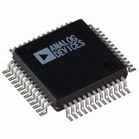
ADUC843BSZ62-5 Analog Devices Inc, ADUC843BSZ62-5 Datasheet - Page 19

ADUC843BSZ62-5
Manufacturer Part Number
ADUC843BSZ62-5
Description
IC ADC 12BIT W/FLASH MCU 52-MQFP
Manufacturer
Analog Devices Inc
Series
MicroConverter® ADuC8xxr
Datasheet
1.EVAL-ADUC842QS.pdf
(88 pages)
Specifications of ADUC843BSZ62-5
Core Size
8-Bit
Program Memory Size
62KB (62K x 8)
Oscillator Type
Internal
Core Processor
8052
Speed
16.78MHz
Connectivity
I²C, SPI, UART/USART
Peripherals
DMA, PSM, PWM, Temp Sensor, WDT
Number Of I /o
32
Program Memory Type
FLASH
Ram Size
2.25K x 8
Voltage - Supply (vcc/vdd)
4.75 V ~ 5.25 V
Data Converters
A/D 8x12b
Operating Temperature
-40°C ~ 85°C
Package / Case
52-MQFP, 52-PQFP
Controller Family/series
(8052) ADUC
No. Of I/o's
34
Ram Memory Size
2KB
Cpu Speed
16.78MHz
No. Of Timers
3
No. Of Pwm
RoHS Compliant
Package
52MQFP
Device Core
8052
Family Name
ADuC8xx
Maximum Speed
16.78 MHz
Operating Supply Voltage
5 V
Data Bus Width
8 Bit
Number Of Programmable I/os
34
Interface Type
I2C/SPI/UART
On-chip Adc
8-chx12-bit
On-chip Dac
2-chx12-bit
Number Of Timers
3
Lead Free Status / RoHS Status
Lead free / RoHS Compliant
Eeprom Size
-
Lead Free Status / RoHS Status
Lead free / RoHS Compliant
Available stocks
Company
Part Number
Manufacturer
Quantity
Price
Company:
Part Number:
ADUC843BSZ62-5
Manufacturer:
AD
Quantity:
1 091
Company:
Part Number:
ADUC843BSZ62-5
Manufacturer:
ADI
Quantity:
170
Company:
Part Number:
ADUC843BSZ62-5
Manufacturer:
Analog Devices Inc
Quantity:
10 000
MEMORY ORGANIZATION
The ADuC841/ADuC842/ADuC843 each contain four different
memory blocks:
•
•
•
•
Flash/EE Program Memory
The parts provide up to 62 kBytes of Flash/EE program mem-
ory to run user code. The user can run code from this internal
memory only. Unlike the ADuC812, where code execution can
overflow from the internal code space to external code space
once the PC becomes greater than 1FFFH, the parts do not
support the roll-over from F7FFH in internal code space to
F800H in external code space. Instead, the 2048 bytes between
F800H and FFFFH appear as NOP instructions to user code.
This internal code space can be downloaded via the UART
serial port while the device is in-circuit. 56 kBytes of the
program memory can be reprogrammed during run time; thus
the code space can be upgraded in the field by using a user
defined protocol, or it can be used as a data memory. This is
discussed in more detail in the Flash/EE Memory section.
For the 32 kBytes memory model, the top 8 kBytes function as
the ULOAD space; this is explained in the Flash/EE Memory
section.
Flash/EE Data Memory
4 kBytes of Flash/EE data memory are available to the user and
can be accessed indirectly via a group of control registers
mapped into the special function register (SFR) area. Access to
the Flash/EE data memory is discussed in detail in the Flash/EE
Memory section.
General-Purpose RAM
The general-purpose RAM is divided into two separate
memories: the upper and the lower 128 bytes of RAM. The
lower 128 bytes of RAM can be accessed through direct or
indirect addressing. The upper 128 bytes of RAM can be
accessed only through indirect addressing because it shares the
same address space as the SFR space, which can be accessed
only through direct addressing.
Up to 62 kBytes of on-chip Flash/EE program memory
4 kBytes of on-chip Flash/EE data memory
256 bytes of general-purpose RAM
2 kBytes of internal XRAM
Rev. 0 | Page 19 of 88
The lower 128 bytes of internal data memory are mapped as
shown in Figure 23. The lowest 32 bytes are grouped into four
banks of eight registers addressed as R0 to R7. The next 16 bytes
(128 bits), locations 20H to 2FH above the register banks, form
a block of directly addressable bit locations at Bit Addresses
00H to 7FH. The stack can be located anywhere in the internal
memory address space, and the stack depth can be expanded up
to 2048 bytes.
Reset initializes the stack pointer to location 07H and incre-
ments it once before loading the stack to start from location
08H, which is also the first register (R0) of register bank 1. Thus,
if the user needs to use more than one register bank, the stack
pointer should be initialized to an area of RAM not used for
data storage.
The parts contain 2048 bytes of internal XRAM, 1792 bytes of
which can be configured to an extended 11-bit stack pointer.
By default, the stack operates exactly like an 8052 in that it rolls
over from FFH to 00H in the general-purpose RAM. On the
parts, however, it is possible (by setting CFG841.7 or CFG842.7)
to enable the 11-bit extended stack pointer. In this case, the
stack rolls over from FFH in RAM to 0100H in XRAM.
The 11-bit stack pointer is visible in the SP and SPH SFRs. The
SP SFR is located at 81H as with a standard 8052. The SPH SFR
is located at B7H. The 3 LSBs of this SFR contain the 3 extra bits
necessary to extend the 8-bit stack pointer into an 11-bit stack
pointer.
BITS IN PSW
SELECTED
BANKS
VIA
Figure 23. Lower 128 Bytes of Internal Data Memory
10
11
01
00
30H
20H
18H
10H
08H
00H
ADuC841/ADuC842/ADuC843
7FH
2FH
1FH
17H
0FH
07H
FOUR BANKS OF EIGHT
REGISTERS
R0 TO R7
BIT-ADDRESSABLE
(BIT ADDRESSES)
GENERAL-PURPOSE
AREA
RESET VALUE OF
STACK POINTER


