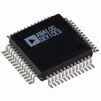
ADUC843BSZ62-5 Analog Devices Inc, ADUC843BSZ62-5 Datasheet - Page 23

ADUC843BSZ62-5
Manufacturer Part Number
ADUC843BSZ62-5
Description
IC ADC 12BIT W/FLASH MCU 52-MQFP
Manufacturer
Analog Devices Inc
Series
MicroConverter® ADuC8xxr
Datasheet
1.EVAL-ADUC842QS.pdf
(88 pages)
Specifications of ADUC843BSZ62-5
Core Size
8-Bit
Program Memory Size
62KB (62K x 8)
Oscillator Type
Internal
Core Processor
8052
Speed
16.78MHz
Connectivity
I²C, SPI, UART/USART
Peripherals
DMA, PSM, PWM, Temp Sensor, WDT
Number Of I /o
32
Program Memory Type
FLASH
Ram Size
2.25K x 8
Voltage - Supply (vcc/vdd)
4.75 V ~ 5.25 V
Data Converters
A/D 8x12b
Operating Temperature
-40°C ~ 85°C
Package / Case
52-MQFP, 52-PQFP
Controller Family/series
(8052) ADUC
No. Of I/o's
34
Ram Memory Size
2KB
Cpu Speed
16.78MHz
No. Of Timers
3
No. Of Pwm
RoHS Compliant
Package
52MQFP
Device Core
8052
Family Name
ADuC8xx
Maximum Speed
16.78 MHz
Operating Supply Voltage
5 V
Data Bus Width
8 Bit
Number Of Programmable I/os
34
Interface Type
I2C/SPI/UART
On-chip Adc
8-chx12-bit
On-chip Dac
2-chx12-bit
Number Of Timers
3
Lead Free Status / RoHS Status
Lead free / RoHS Compliant
Eeprom Size
-
Lead Free Status / RoHS Status
Lead free / RoHS Compliant
Available stocks
Company
Part Number
Manufacturer
Quantity
Price
Company:
Part Number:
ADUC843BSZ62-5
Manufacturer:
AD
Quantity:
1 091
Company:
Part Number:
ADUC843BSZ62-5
Manufacturer:
ADI
Quantity:
170
Company:
Part Number:
ADUC843BSZ62-5
Manufacturer:
Analog Devices Inc
Quantity:
10 000
ADC CIRCUIT INFORMATION
General Overview
The ADC conversion block incorporates a fast, 8-channel,
12-bit, single-supply ADC. This block provides the user with
multichannel mux, track-and-hold, on-chip reference, calibra-
tion features, and ADC. All components in this block are easily
configured via a 3-register SFR interface.
The ADC converter consists of a conventional successive
approximation converter based around a capacitor DAC. The
converter accepts an analog input range of 0 V to V
precision, 15 ppm, low drift, factory calibrated 2.5 V reference is
provided on-chip. An external reference can be connected as
described in the Voltage Reference Connections section. This
external reference can be in the range 1 V to AV
Single-step or continuous conversion modes can be initiated in
software or alternatively by applying a convert signal to an
external pin. Timer 2 can also be configured to generate a
repetitive trigger for ADC conversions. The ADC may be
configured to operate in a DMA mode whereby the ADC block
continuously converts and captures samples to an external
RAM space without any interaction from the MCU core. This
automatic capture facility can extend through a 16 MByte
external data memory space.
The ADuC841/ADuC842/ADuC843 are shipped with factory
programmed calibration coefficients that are automatically
downloaded to the ADC on power-up, ensuring optimum ADC
performance. The ADC core contains internal offset and gain
calibration registers that can be hardware calibrated to
minimize system errors.
A voltage output from an on-chip band gap reference propor-
tional to absolute temperature can also be routed through the
front end ADC multiplexer (effectively a 9th ADC channel
input), facilitating a temperature sensor implementation.
DD
.
REF
. A high
Rev. 0 | Page 23 of 88
ADC Transfer Function
The analog input range for the ADC is 0 V to V
range, the designed code transitions occur midway between
successive integer LSB values, i.e., 0.5 LSB, 1.5 LSB, 2.5 LSB . . .
FS –1.5 LSB. The output coding is straight binary with 1 LSB =
FS/4096 or 2.5 V/4096 = 0.61 mV when V
input/output transfer characteristic for the 0 V to V
shown in Figure 28.
Typical Operation
Once configured via the ADCCON 1–3 SFRs, the ADC converts
the analog input and provides an ADC 12-bit result word in the
ADCDATAH/L SFRs. The top 4 bits of the ADCDATAH SFR
are written with the channel selection bits to identify the channel
result. The format of the ADC 12-bit result word is shown in
Figure 29.
TOP 4 BITS
CH–ID
111...101
000...010
111...111
111...110
111...100
000...011
000...001
000...000
OUTPUT
CODE
0V 1LSB
Figure 29. ADC Result Word Format
Figure 28. ADC Transfer Function
1LSB =
ADuC841/ADuC842/ADuC843
4096
FS
LOW 8 BITS OF THE
ADC RESULT WORD
HIGH 4 BITS OF
ADC RESULT WORD
REF
= 2.5 V. The ideal
+FS
ADCDATAH SFR
ADCDATAL SFR
REF
. For this
REF
range is


