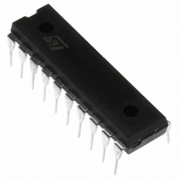
ST7FLITE29F2B6 STMicroelectronics, ST7FLITE29F2B6 Datasheet - Page 46

ST7FLITE29F2B6
Manufacturer Part Number
ST7FLITE29F2B6
Description
IC MCU 8BIT 8K FLASH 20DIP
Manufacturer
STMicroelectronics
Series
ST7r
Datasheet
1.ST7FLITE20F2B6.pdf
(133 pages)
Specifications of ST7FLITE29F2B6
Core Processor
ST7
Core Size
8-Bit
Speed
8MHz
Connectivity
SPI
Peripherals
LVD, POR, PWM, WDT
Number Of I /o
15
Program Memory Size
8KB (8K x 8)
Program Memory Type
FLASH
Eeprom Size
256 x 8
Ram Size
384 x 8
Voltage - Supply (vcc/vdd)
2.4 V ~ 5.5 V
Data Converters
A/D 7x10b
Oscillator Type
Internal
Operating Temperature
-40°C ~ 85°C
Package / Case
20-DIP (0.300", 7.62mm)
Processor Series
ST7FLITE2x
Core
ST7
Data Bus Width
8 bit
Data Ram Size
384 B
Interface Type
SPI
Maximum Clock Frequency
8 MHz
Number Of Programmable I/os
15
Number Of Timers
4 bit
Operating Supply Voltage
2.4 V to 5.5 V
Maximum Operating Temperature
+ 85 C
Mounting Style
Through Hole
Development Tools By Supplier
ST7FLIT2-COS/COM, ST7FLITE-SK/RAIS, ST7MDT10-DVP3, ST7MDT10-EMU3, STX-RLINK
Minimum Operating Temperature
- 40 C
On-chip Adc
13 bit
For Use With
497-5858 - EVAL BOARD PLAYBACK ST7FLITE497-5049 - KIT STARTER RAISONANCE ST7FLITE497-5046 - KIT TOOL FOR ST7/UPSD/STR7 MCU
Lead Free Status / RoHS Status
Lead free / RoHS Compliant
Other names
497-2134-5
Available stocks
Company
Part Number
Manufacturer
Quantity
Price
Part Number:
ST7FLITE29F2B6
Manufacturer:
ST
Quantity:
20 000
ST7LITE2
10 I/O PORTS
10.1 INTRODUCTION
The I/O ports allow data transfer. An I/O port can
contain up to 8 pins. Each pin can be programmed
independently either as a digital input or digital
output. In addition, specific pins may have several
other functions. These functions can include exter-
nal interrupt, alternate signal input/output for on-
chip peripherals or analog input.
10.2 FUNCTIONAL DESCRIPTION
A Data Register (DR) and a Data Direction Regis-
ter (DDR) are always associated with each port.
The Option Register (OR), which allows input/out-
put options, may or may not be implemented. The
following description takes into account the OR
register. Refer to the Port Configuration table for
device specific information.
An I/O pin is programmed using the corresponding
bits in the DDR, DR and OR registers: bit x corre-
sponding to pin x of the port.
Figure 31
10.2.1 Input Modes
Clearing the DDRx bit selects input mode. In this
mode, reading its DR bit returns the digital value
from that I/O pin.
If an OR bit is available, different input modes can
be configured by software: floating or pull-up. Re-
fer to I/O Port Implementation section for configu-
ration.
Notes:
1. Writing to the DR modifies the latch value but
does not change the state of the input pin.
2. Do not use read/modify/write instructions
(BSET/BRES) to modify the DR register.
10.2.1.1 External Interrupt Function
Depending on the device, setting the ORx bit while
in input mode can configure an I/O as an input with
interrupt. In this configuration, a signal edge or lev-
el input on the I/O generates an interrupt request
via the corresponding interrupt vector (eix).
Falling or rising edge sensitivity is programmed in-
dependently for each interrupt vector. The Exter-
nal Interrupt Control Register (EICR) or the Miscel-
laneous Register controls this sensitivity, depend-
ing on the device.
Each external interrupt vector is linked to a dedi-
cated group of I/O port pins (see pinout description
in
46/133
1
section 2 on page 6
shows the generic I/O block diagram.
and interrupt section).
If several I/O interrupt pins on the same interrupt
vector are selected simultaneously, they are logi-
cally combined. For this reason if one of the inter-
rupt pins is tied low, it may mask the others.
External interrupts are hardware interrupts. Fetch-
ing the corresponding interrupt vector automatical-
ly clears the request latch. Changing the sensitivity
of a particular external interrupt clears this pending
interrupt. This can be used to clear unwanted
pending interrupts.
Spurious interrupts
When enabling/disabling an external interrupt by
setting/resetting the related OR register bit, a spu-
rious interrupt is generated if the pin level is low
and its edge sensitivity includes falling/rising edge.
This is due to the edge detector input which is
switched to '1' when the external interrupt is disa-
bled by the OR register.
To avoid this unwanted interrupt, a "safe" edge
sensitivity (rising edge for enabling and falling
edge for disabling) has to be selected before
changing the OR register bit and configuring the
appropriate sensitivity again.
Caution: In case a pin level change occurs during
these operations (asynchronous signal input), as
interrupts are generated according to the current
sensitivity, it is advised to disable all interrupts be-
fore and to reenable them after the complete pre-
vious sequence in order to avoid an external inter-
rupt occurring on the unwanted edge.
This corresponds to the following steps:
1. To enable an external interrupt:
2. To disable an external interrupt:
– set the interrupt mask with the SIM instruction
– select rising edge
– enable the external interrupt through the OR
– select the desired sensitivity if different from
– reset the interrupt mask with the RIM instruc-
– set the interrupt mask with the SIM instruction
– select falling edge
(in cases where a pin level change could oc-
cur)
register
rising edge
tion (in cases where a pin level change could
occur)
SIM (in cases where a pin level change could
occur)


