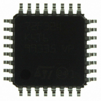
ST72F324K4T6 STMicroelectronics, ST72F324K4T6 Datasheet - Page 140

ST72F324K4T6
Manufacturer Part Number
ST72F324K4T6
Description
MCU 8BIT 16K FLASH 5V 32LQFP
Manufacturer
STMicroelectronics
Series
ST7r
Datasheet
1.ST72F324J2T6.pdf
(164 pages)
Specifications of ST72F324K4T6
Core Processor
ST7
Core Size
8-Bit
Speed
8MHz
Connectivity
SCI, SPI
Peripherals
LVD, POR, PWM, WDT
Number Of I /o
24
Program Memory Size
16KB (16K x 8)
Program Memory Type
FLASH
Ram Size
512 x 8
Voltage - Supply (vcc/vdd)
3.8 V ~ 5.5 V
Data Converters
A/D 12x10b
Oscillator Type
Internal
Operating Temperature
-40°C ~ 85°C
Package / Case
32-LQFP
Processor Series
ST72F3x
Core
ST7
Data Bus Width
8 bit
Data Ram Size
512 B
Interface Type
SCI, SPI
Maximum Clock Frequency
8 MHz
Number Of Programmable I/os
32
Number Of Timers
4 bit
Operating Supply Voltage
3.8 V to 5.5 V
Maximum Operating Temperature
+ 85 C
Mounting Style
SMD/SMT
Development Tools By Supplier
ST7F521-IND/USB, ST7232X-EVAL, ST7MDT20-DVP3, ST7MDT20J-EMU3, STX-RLINK
Minimum Operating Temperature
- 40 C
On-chip Adc
10 bit
For Use With
497-6421 - BOARD EVAL DGTL BATT CHGR DESIGN497-5046 - KIT TOOL FOR ST7/UPSD/STR7 MCU
Lead Free Status / RoHS Status
Lead free / RoHS Compliant
Eeprom Size
-
Lead Free Status / Rohs Status
In Transition
Other names
497-4851
Available stocks
Company
Part Number
Manufacturer
Quantity
Price
Company:
Part Number:
ST72F324K4T6
Manufacturer:
ST
Quantity:
1 000
Company:
Part Number:
ST72F324K4T6
Manufacturer:
STMicroelectronics
Quantity:
10 000
Part Number:
ST72F324K4T6
Manufacturer:
ST
Quantity:
20 000
Company:
Part Number:
ST72F324K4T6TR
Manufacturer:
STM
Quantity:
4 822
Company:
Part Number:
ST72F324K4T6TR
Manufacturer:
STMicroelectronics
Quantity:
10 000
ST72324Jx ST72324Kx
12.12 COMMUNICATION INTERFACE CHARACTERISTICS
12.12.1 SPI - Serial Peripheral Interface
Subject to general operating conditions for V
design simulation and/or characterisation results, not tested in production.
When no communication is on-going the data output line of the SPI (MOSI in master mode, MISO in slave
mode) has its alternate function capability released. In this case, the pin status depends on the I/O port
configuration. Refer to I/O port characteristics for more details on the input/output alternate function char-
acteristics (SS, SCK, MOSI, MISO).
Figure 80. SPI Slave Timing Diagram with CPHA=0
Notes:
1. Measurement points are done at CMOS levels: 0.3xV
140/164
1
Symbol
1/t
t
t
w(SCKH)
w(SCKL)
t
t
t
t
t
t
t
t
dis(SO)
t
t
t
t
r(SCK)
su(SS)
f(SCK)
t
su(MI)
t
v(MO)
h(MO)
f
su(SI)
a(SO)
v(SO)
h(SO)
MISO
MOSI
h(SS)
h(MI)
c(SCK)
h(SI)
SCK
SS
CPHA=0
CPOL=0
CPHA=0
CPOL=1
OUTPUT
INPUT
INPUT
SPI clock frequency
SPI clock rise and fall time
SS setup time
SS hold time
SCK high and low time
Data input setup time
Data input hold time
Data output access time
Data output disable time
Data output valid time
Data output hold time
Data output valid time
Data output hold time
see note 2
t
a(SO)
t
su(SS)
t
su(SI)
Parameter
t
t
MSB IN
w(SCKH)
w(SCKL)
MSB OUT
t
t
h(SI)
c(SCK)
DD
t
v(SO)
, f
DD
CPU
Slave
Master
Slave
Slave
Slave
Master
Slave
Master
Slave
Master
Slave
Slave
Slave (after enable edge)
Master (before capture edge)
BIT6 OUT
and 0.7xV
, and T
1)
Conditions
A
DD
unless otherwise specified. Data based on
BIT1 IN
.
t
f
f
h(SO)
CPU
CPU
=8MHz
=8MHz
t
t
r(SCK)
f(SCK)
f
CPU
LSB IN
0.0625
see I/O port pin description
0.25
0.25
Min
120
120
100
100
100
100
100
90
LSB OUT
0
0
0
/128
t
h(SS)
f
f
CPU
CPU
Max
120
240
90
2
4
/4
/2
t
dis(SO)
Unit
t
MHz
CPU
ns
note 2
see


