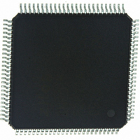
Z16F2811AL20SG Zilog, Z16F2811AL20SG Datasheet - Page 198

Z16F2811AL20SG
Manufacturer Part Number
Z16F2811AL20SG
Description
IC ZNEO MCU FLASH 128K 100LQFP
Manufacturer
Zilog
Series
Encore!® ZNEOr
Specifications of Z16F2811AL20SG
Core Processor
ZNEO
Core Size
16-Bit
Speed
20MHz
Connectivity
EBI/EMI, I²C, IrDA, LIN, SPI, UART/USART
Peripherals
Brown-out Detect/Reset, DMA, POR, PWM, WDT
Number Of I /o
76
Program Memory Size
128KB (128K x 8)
Program Memory Type
FLASH
Ram Size
4K x 8
Voltage - Supply (vcc/vdd)
2.7 V ~ 3.6 V
Data Converters
A/D 12x10b
Oscillator Type
Internal
Operating Temperature
0°C ~ 70°C
Package / Case
100-LQFP
Processor Series
Z16F2x
Core
Zneo
Data Bus Width
16 bit
Data Ram Size
4 B
Interface Type
ESPI, I2C, UART
Maximum Clock Frequency
20 MHz
Number Of Programmable I/os
76
Number Of Timers
4
Operating Supply Voltage
2.7 V to 3.6 V
Maximum Operating Temperature
+ 70 C
Mounting Style
SMD/SMT
Development Tools By Supplier
Z16F2800100ZCOG
Minimum Operating Temperature
0 C
On-chip Adc
10 bit, 12 Channel
For Use With
770-1003 - ISP 4PORT FOR ZILOG ZNEO MCU269-4537 - DEV KIT FOR Z16F ZNEO
Lead Free Status / RoHS Status
Lead free / RoHS Compliant
Eeprom Size
-
Lead Free Status / Rohs Status
Details
Other names
269-4533
Available stocks
Company
Part Number
Manufacturer
Quantity
Price
Company:
Part Number:
Z16F2811AL20SG
Manufacturer:
VISHAY
Quantity:
9 487
Part Number:
Z16F2811AL20SG
Manufacturer:
ZILOG
Quantity:
20 000
- Current page: 198 of 388
- Download datasheet (22Mb)
PS022008-0810
Input Sample Time
Modes of Operation
(CLKPOL = 0)
(CLKPOL = 1)
This section describes the different modes of data transfer supported by the ESPI block.
The mode is selected by the slave select mode (SSMD) field of the mode register.
SPI Mode
This mode is selected by setting the SSMD field of the mode Register to 000. In this
mode, software or DMA controls the assertion of the SS signal directly via the SSV bit of
the SPI transmit data command register. Either DMA or software is used to control an SPI
mode transaction. Prior to or simultaneously with writing the first transmit data byte,
software or DMA sets the SSV bit. Software sets the SSV bit either by performing a byte
write to the transmit data command register prior to writing the first transmit character to
the data register or by performing a word write to the data register address which loads the
first transmit character and simultaneously sets the SSV bit.
The DMA sets the SSV bit via the command field of the descriptor. The SSV bit is written
on the DMA command bus prior to or in sync with the first data byte. SS will remain
asserted while one or more characters are transferred. There are two mechanisms for
deasserting SS at the end of the transaction. One method is used by DMA and also by
MOSI
MISO
SCK
SCK
SS
Figure 36. ESPI Timing when
Bit7
Bit7
Bit6
Bit6
P R E L I M I N A R Y
Bit5
Bit5
Bit4
Bit4
PHASE
Bit3
Bit3
Enhanced Serial Peripheral Interface
= 1
Bit2
Bit2
Product Specification
ZNEO
Bit1
Bit1
Bit0
Bit0
Z16F Series
182
Related parts for Z16F2811AL20SG
Image
Part Number
Description
Manufacturer
Datasheet
Request
R

Part Number:
Description:
High Performance Microcontrollers
Manufacturer:
ZiLOG Semiconductor
Datasheet:

Part Number:
Description:
Communication Controllers, ZILOG INTELLIGENT PERIPHERAL CONTROLLER (ZIP)
Manufacturer:
Zilog, Inc.
Datasheet:

Part Number:
Description:
KIT DEV FOR Z8 ENCORE 16K TO 64K
Manufacturer:
Zilog
Datasheet:

Part Number:
Description:
KIT DEV Z8 ENCORE XP 28-PIN
Manufacturer:
Zilog
Datasheet:

Part Number:
Description:
DEV KIT FOR Z8 ENCORE 8K/4K
Manufacturer:
Zilog
Datasheet:

Part Number:
Description:
KIT DEV Z8 ENCORE XP 28-PIN
Manufacturer:
Zilog
Datasheet:

Part Number:
Description:
DEV KIT FOR Z8 ENCORE 4K TO 8K
Manufacturer:
Zilog
Datasheet:

Part Number:
Description:
CMOS Z8 microcontroller. ROM 16 Kbytes, RAM 256 bytes, speed 16 MHz, 32 lines I/O, 3.0V to 5.5V
Manufacturer:
Zilog, Inc.
Datasheet:

Part Number:
Description:
Low-cost microcontroller. 512 bytes ROM, 61 bytes RAM, 8 MHz
Manufacturer:
Zilog, Inc.
Datasheet:

Part Number:
Description:
Z8 4K OTP Microcontroller
Manufacturer:
Zilog, Inc.
Datasheet:

Part Number:
Description:
CMOS SUPER8 ROMLESS MCU
Manufacturer:
Zilog, Inc.
Datasheet:

Part Number:
Description:
SL1866 CMOSZ8 OTP Microcontroller
Manufacturer:
Zilog, Inc.
Datasheet:

Part Number:
Description:
SL1866 CMOSZ8 OTP Microcontroller
Manufacturer:
Zilog, Inc.
Datasheet:

Part Number:
Description:
OTP (KB) = 1, RAM = 125, Speed = 12, I/O = 14, 8-bit Timers = 2, Comm Interfaces Other Features = Por, LV Protect, Voltage = 4.5-5.5V
Manufacturer:
Zilog, Inc.
Datasheet:


