C8051F819-GM Silicon Laboratories Inc, C8051F819-GM Datasheet - Page 11
C8051F819-GM
Manufacturer Part Number
C8051F819-GM
Description
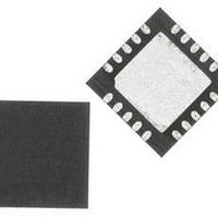
IC MCU 8BIT 8KB FLASH 20QFN
Manufacturer
Silicon Laboratories Inc
Series
C8051F81xr
Datasheet
1.C8051F800DK.pdf
(250 pages)
Specifications of C8051F819-GM
Core Processor
8051
Core Size
8-Bit
Speed
25MHz
Connectivity
SMBus (2-Wire/I²C), SPI, UART/USART
Peripherals
Cap Sense, POR, PWM, WDT
Number Of I /o
17
Program Memory Size
8KB (8K x 8)
Program Memory Type
FLASH
Ram Size
512 x 8
Voltage - Supply (vcc/vdd)
1.8 V ~ 3.6 V
Oscillator Type
Internal
Operating Temperature
-40°C ~ 85°C
Package / Case
20-QFN
Processor Series
C8051F8x
Core
8051
Data Bus Width
16 bit
Data Ram Size
512 B
Interface Type
I2C, SPI, UART
Maximum Clock Frequency
25 MHz
Number Of Programmable I/os
17
Number Of Timers
3
Operating Supply Voltage
1.8 V to 3.6 V
Maximum Operating Temperature
+ 125 C
Mounting Style
SMD/SMT
3rd Party Development Tools
PK51, CA51, A51, ULINK2
Development Tools By Supplier
C8051F800DK
Minimum Operating Temperature
- 55 C
Package
20QFN EP
Device Core
8051
Family Name
C8051F8xx
Maximum Speed
25 MHz
Lead Free Status / RoHS Status
Lead free / RoHS Compliant
Eeprom Size
-
Data Converters
-
Lead Free Status / Rohs Status
Details
Other names
336-1799-5


27. UART0
28. Timers
29. Programmable Counter Array
30. C2 Interface
Figure 26.3. SMBus Transaction ........................................................................... 182
Figure 26.4. Typical SMBus SCL Generation ........................................................ 184
Figure 26.5. Typical Master Write Sequence ........................................................ 193
Figure 26.6. Typical Master Read Sequence ........................................................ 194
Figure 26.7. Typical Slave Write Sequence .......................................................... 195
Figure 26.8. Typical Slave Read Sequence .......................................................... 196
Figure 27.1. UART0 Block Diagram ...................................................................... 201
Figure 27.2. UART0 Baud Rate Logic ................................................................... 202
Figure 27.3. UART Interconnect Diagram ............................................................. 203
Figure 27.4. 8-Bit UART Timing Diagram .............................................................. 203
Figure 27.5. 9-Bit UART Timing Diagram .............................................................. 204
Figure 27.6. UART Multi-Processor Mode Interconnect Diagram ......................... 205
Figure 28.1. T0 Mode 0 Block Diagram ................................................................. 212
Figure 28.2. T0 Mode 2 Block Diagram ................................................................. 213
Figure 28.3. T0 Mode 3 Block Diagram ................................................................. 214
Figure 28.4. Timer 2 16-Bit Mode Block Diagram ................................................. 219
Figure 28.5. Timer 2 8-Bit Mode Block Diagram ................................................... 220
Figure 29.1. PCA Block Diagram ........................................................................... 225
Figure 29.2. PCA Counter/Timer Block Diagram ................................................... 226
Figure 29.3. PCA Interrupt Block Diagram ............................................................ 227
Figure 29.4. PCA Capture Mode Diagram ............................................................. 229
Figure 29.5. PCA Software Timer Mode Diagram ................................................. 230
Figure 29.6. PCA High-Speed Output Mode Diagram ........................................... 231
Figure 29.7. PCA Frequency Output Mode ........................................................... 232
Figure 29.8. PCA 8-Bit PWM Mode Diagram ........................................................ 233
Figure 29.9. PCA 9-bit through 15-Bit PWM Mode Diagram ................................. 234
Figure 29.10. PCA 16-Bit PWM Mode ................................................................... 235
Figure 29.11. PCA Module 2 with Watchdog Timer Enabled ................................ 236
Figure 30.1. Typical C2 Pin Sharing ...................................................................... 247
Rev. 1.0
C8051F80x-83x
11
Related parts for C8051F819-GM
Image
Part Number
Description
Manufacturer
Datasheet
Request
R

Part Number:
Description:
SMD/C°/SINGLE-ENDED OUTPUT SILICON OSCILLATOR
Manufacturer:
Silicon Laboratories Inc
Part Number:
Description:
Manufacturer:
Silicon Laboratories Inc
Datasheet:
Part Number:
Description:
N/A N/A/SI4010 AES KEYFOB DEMO WITH LCD RX
Manufacturer:
Silicon Laboratories Inc
Datasheet:
Part Number:
Description:
N/A N/A/SI4010 SIMPLIFIED KEY FOB DEMO WITH LED RX
Manufacturer:
Silicon Laboratories Inc
Datasheet:
Part Number:
Description:
N/A/-40 TO 85 OC/EZLINK MODULE; F930/4432 HIGH BAND (REV E/B1)
Manufacturer:
Silicon Laboratories Inc
Part Number:
Description:
EZLink Module; F930/4432 Low Band (rev e/B1)
Manufacturer:
Silicon Laboratories Inc
Part Number:
Description:
I°/4460 10 DBM RADIO TEST CARD 434 MHZ
Manufacturer:
Silicon Laboratories Inc
Part Number:
Description:
I°/4461 14 DBM RADIO TEST CARD 868 MHZ
Manufacturer:
Silicon Laboratories Inc
Part Number:
Description:
I°/4463 20 DBM RFSWITCH RADIO TEST CARD 460 MHZ
Manufacturer:
Silicon Laboratories Inc
Part Number:
Description:
I°/4463 20 DBM RADIO TEST CARD 868 MHZ
Manufacturer:
Silicon Laboratories Inc
Part Number:
Description:
I°/4463 27 DBM RADIO TEST CARD 868 MHZ
Manufacturer:
Silicon Laboratories Inc
Part Number:
Description:
I°/4463 SKYWORKS 30 DBM RADIO TEST CARD 915 MHZ
Manufacturer:
Silicon Laboratories Inc
Part Number:
Description:
N/A N/A/-40 TO 85 OC/4463 RFMD 30 DBM RADIO TEST CARD 915 MHZ
Manufacturer:
Silicon Laboratories Inc
Part Number:
Description:
I°/4463 20 DBM RADIO TEST CARD 169 MHZ
Manufacturer:
Silicon Laboratories Inc