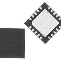
C8051F819-GM Silicon Laboratories Inc, C8051F819-GM Datasheet - Page 244

C8051F819-GM
Manufacturer Part Number
C8051F819-GM
Description
IC MCU 8BIT 8KB FLASH 20QFN
Manufacturer
Silicon Laboratories Inc
Series
C8051F81xr
Datasheet
1.C8051F800DK.pdf
(250 pages)
Specifications of C8051F819-GM
Core Processor
8051
Core Size
8-Bit
Speed
25MHz
Connectivity
SMBus (2-Wire/I²C), SPI, UART/USART
Peripherals
Cap Sense, POR, PWM, WDT
Number Of I /o
17
Program Memory Size
8KB (8K x 8)
Program Memory Type
FLASH
Ram Size
512 x 8
Voltage - Supply (vcc/vdd)
1.8 V ~ 3.6 V
Oscillator Type
Internal
Operating Temperature
-40°C ~ 85°C
Package / Case
20-QFN
Processor Series
C8051F8x
Core
8051
Data Bus Width
16 bit
Data Ram Size
512 B
Interface Type
I2C, SPI, UART
Maximum Clock Frequency
25 MHz
Number Of Programmable I/os
17
Number Of Timers
3
Operating Supply Voltage
1.8 V to 3.6 V
Maximum Operating Temperature
+ 125 C
Mounting Style
SMD/SMT
3rd Party Development Tools
PK51, CA51, A51, ULINK2
Development Tools By Supplier
C8051F800DK
Minimum Operating Temperature
- 55 C
Package
20QFN EP
Device Core
8051
Family Name
C8051F8xx
Maximum Speed
25 MHz
Lead Free Status / RoHS Status
Lead free / RoHS Compliant
Eeprom Size
-
Data Converters
-
Lead Free Status / Rohs Status
Details
Other names
336-1799-5
- Current page: 244 of 250
- Download datasheet (2Mb)
C8051F80x-83x
30. C2 Interface
C8051F80x-83x devices include an on-chip Silicon Labs 2-Wire (C2) debug interface to allow Flash pro-
gramming and in-system debugging with the production part installed in the end application. The C2 inter-
face operates using only two pins: a bi-directional data signal (C2D), and a clock input (C2CK). See the C2
Interface Specification for details on the C2 protocol.
30.1. C2 Interface Registers
The following describes the C2 registers necessary to perform Flash programming functions through the
C2 interface. All C2 registers are accessed through the C2 interface as described in the C2 Interface Spec-
ification.
C2 Register Definition 30.1. C2ADD: C2 Address
244
*Note: CRC registers and functions are described in
Name
Reset
7:0 C2ADD[7:0] C2 Address.
Bit
Type
Bit
page 159
Name
7
0
.
The C2ADD register is accessed via the C2 interface to select the target Data register
for C2 Data Read and Data Write commands.
Address
0x00
0x01
0x02
0xBF
0xD2
0xD3
0xCE
0xDE
0xCF
0xDD
6
0
Name
DEVICEID
REVID
FPCTL
FPDAT
CRC0AUTO* Selects the CRC0AUTO Register
CRC0CNT*
CRC0CN*
CRC0DATA*
CRC0FLIP*
CRC0IN*
5
0
Selects the CRC0FLIP Register
Description
Selects the Device ID Register (read only)
Selects the Revision ID Register (read only)
Selects the C2 Flash Programming Control Register
Selects the C2 Flash Data Register
Selects the CRC0CNT Register
Selects the CRC0CN Register
Selects the CRC0DATA Register
Selects the CRC0IN Register
Section “24. Cyclic Redundancy Check Unit (CRC0)” on
Rev. 1.0
4
0
C2ADD[7:0]
R/W
Function
3
0
2
0
1
0
0
0
Related parts for C8051F819-GM
Image
Part Number
Description
Manufacturer
Datasheet
Request
R
Part Number:
Description:
SMD/C°/SINGLE-ENDED OUTPUT SILICON OSCILLATOR
Manufacturer:
Silicon Laboratories Inc
Part Number:
Description:
Manufacturer:
Silicon Laboratories Inc
Datasheet:
Part Number:
Description:
N/A N/A/SI4010 AES KEYFOB DEMO WITH LCD RX
Manufacturer:
Silicon Laboratories Inc
Datasheet:
Part Number:
Description:
N/A N/A/SI4010 SIMPLIFIED KEY FOB DEMO WITH LED RX
Manufacturer:
Silicon Laboratories Inc
Datasheet:
Part Number:
Description:
N/A/-40 TO 85 OC/EZLINK MODULE; F930/4432 HIGH BAND (REV E/B1)
Manufacturer:
Silicon Laboratories Inc
Part Number:
Description:
EZLink Module; F930/4432 Low Band (rev e/B1)
Manufacturer:
Silicon Laboratories Inc
Part Number:
Description:
I°/4460 10 DBM RADIO TEST CARD 434 MHZ
Manufacturer:
Silicon Laboratories Inc
Part Number:
Description:
I°/4461 14 DBM RADIO TEST CARD 868 MHZ
Manufacturer:
Silicon Laboratories Inc
Part Number:
Description:
I°/4463 20 DBM RFSWITCH RADIO TEST CARD 460 MHZ
Manufacturer:
Silicon Laboratories Inc
Part Number:
Description:
I°/4463 20 DBM RADIO TEST CARD 868 MHZ
Manufacturer:
Silicon Laboratories Inc
Part Number:
Description:
I°/4463 27 DBM RADIO TEST CARD 868 MHZ
Manufacturer:
Silicon Laboratories Inc
Part Number:
Description:
I°/4463 SKYWORKS 30 DBM RADIO TEST CARD 915 MHZ
Manufacturer:
Silicon Laboratories Inc
Part Number:
Description:
N/A N/A/-40 TO 85 OC/4463 RFMD 30 DBM RADIO TEST CARD 915 MHZ
Manufacturer:
Silicon Laboratories Inc
Part Number:
Description:
I°/4463 20 DBM RADIO TEST CARD 169 MHZ
Manufacturer:
Silicon Laboratories Inc


