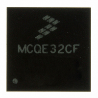
MC9S08QE32CFT Freescale Semiconductor, MC9S08QE32CFT Datasheet - Page 21

MC9S08QE32CFT
Manufacturer Part Number
MC9S08QE32CFT
Description
MCU 8BIT 32K FLASH 48-QFN
Manufacturer
Freescale Semiconductor
Series
HCS08r
Specifications of MC9S08QE32CFT
Core Processor
HCS08
Core Size
8-Bit
Speed
50MHz
Connectivity
I²C, LIN, SCI, SPI
Peripherals
LVD, PWM, WDT
Number Of I /o
38
Program Memory Size
32KB (32K x 8)
Program Memory Type
FLASH
Ram Size
2K x 8
Voltage - Supply (vcc/vdd)
1.8 V ~ 3.6 V
Data Converters
A/D 10x12b
Oscillator Type
Internal
Operating Temperature
-40°C ~ 85°C
Package / Case
48-QFN
Cpu Family
HCS08
Device Core Size
8b
Interface Type
SCI/SPI
# I/os (max)
40
Operating Supply Voltage (typ)
3.3V
Operating Supply Voltage (max)
3.6V
Operating Supply Voltage (min)
2V
On-chip Adc
10-chx12-bit
Instruction Set Architecture
CISC
Operating Temp Range
-40C to 85C
Operating Temperature Classification
Industrial
Mounting
Surface Mount
Pin Count
48
Package Type
QFN EP
Processor Series
S08QE
Core
HCS08
Data Bus Width
8 bit
Data Ram Size
2 KB
Number Of Programmable I/os
40
Operating Supply Voltage
- 0.3 V to + 3.8 V
Maximum Operating Temperature
+ 85 C
Mounting Style
SMD/SMT
3rd Party Development Tools
EWS08
Development Tools By Supplier
DEMOQE128, EVBQE128
Minimum Operating Temperature
- 40 C
For Use With
DEMO9S08QE32 - DEMO FOR S08 AND QE32/16DC9S08QE32 - DAUGHTER CARD FOR DEMO9S
Lead Free Status / RoHS Status
Lead free / RoHS Compliant
Eeprom Size
-
Lead Free Status / Rohs Status
Compliant
3.10.2
Synchronizer circuits determine the shortest input pulses that can be recognized or the fastest clock that
can be used as the optional external source to the timer counter. These synchronizers operate from the
current bus rate clock.
Freescale Semiconductor
1
2
3
4
5
Num
Typical values are based on characterization data at V
This is the shortest pulse that is guaranteed to be recognized as a reset pin request. Shorter pulses are not guaranteed to
override reset requests from internal sources.
To enter BDM mode following a POR, BKGD/MS must be held low during the power-up and for a hold time of t
rises above V
This is the minimum pulse width that is guaranteed to pass through the pin synchronization circuitry. Shorter pulses may or
may not be recognized. In stop mode, the synchronizer is bypassed so shorter pulses can be recognized in that case.
Timing is shown with respect to 20% V
10
8
9
C
D
C
C
Keyboard interrupt pulse width
Port rise and fall time —
Low output drive (PTxDS = 0) (load = 50 pF)
Port rise and fall time —
High output drive (PTxDS = 1) (load = 50 pF)
Voltage regulator recovery time
TPM Module Timing
LVD
.
RESET PIN
Slew rate control disabled (PTxSE = 0)
Slew rate control disabled (PTxSE = 0)
Slew rate control enabled (PTxSE = 1)
Slew rate control enabled (PTxSE = 1)
IRQ/KBIPx
Rating
KBIPx
MC9S08QE32 Series MCU Data Sheet, Rev. 6
DD
Table 12. Control Timing (continued)
and 80% V
Figure 14. IRQ/KBIPx Timing
Figure 13. Reset Timing
Asynchronous path
Synchronous path
DD
DD
5
levels. Temperature range –40 °C to 85 °C.
= 3.0 V, 25 °C unless otherwise stated.
t
t
IHIL
ILIH
t
extrst
2
5
t
t
t
Symbol
ILIH,
Rise
Rise
t
VRR
, t
, t
t
IHIL
Fall
Fall
1.5 × t
Min
100
—
—
—
—
—
cyc
Typical
Electrical Characteristics
31
24
—
—
8
7
4
1
Max
—
—
—
—
—
—
—
MSH
after V
Unit
ns
ns
ns
μs
DD
21


