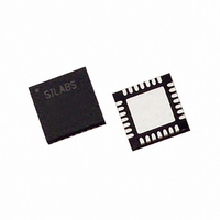
C8051F321-GM Silicon Laboratories Inc, C8051F321-GM Datasheet - Page 67

C8051F321-GM
Manufacturer Part Number
C8051F321-GM
Description
IC 8051 MCU 16K FLASH 28MLP
Manufacturer
Silicon Laboratories Inc
Series
C8051F32xr
Datasheets
1.C8051F320-TB.pdf
(250 pages)
2.C8051F321-GMR.pdf
(2 pages)
3.C8051F321-GM.pdf
(256 pages)
Specifications of C8051F321-GM
Program Memory Type
FLASH
Program Memory Size
16KB (16K x 8)
Package / Case
28-VQFN Exposed Pad, 28-HVQFN, 28-SQFN, 28-DHVQFN
Core Processor
8051
Core Size
8-Bit
Speed
25MHz
Connectivity
SMBus (2-Wire/I²C), SPI, UART/USART, USB
Peripherals
Brown-out Detect/Reset, POR, PWM, Temp Sensor, WDT
Number Of I /o
21
Ram Size
2.25K x 8
Voltage - Supply (vcc/vdd)
2.7 V ~ 3.6 V
Data Converters
A/D 13x10b
Oscillator Type
Internal
Operating Temperature
-40°C ~ 85°C
Processor Series
C8051F3x
Core
8051
Data Bus Width
8 bit
Data Ram Size
2.25 KB
Interface Type
I2C/SMBus/SPI/UART/USB
Maximum Clock Frequency
25 MHz
Number Of Programmable I/os
21
Number Of Timers
4
Operating Supply Voltage
2.7 V to 3.6 V
Maximum Operating Temperature
+ 85 C
Mounting Style
SMD/SMT
3rd Party Development Tools
PK51, CA51, A51, ULINK2
Development Tools By Supplier
C8051F320DK
Minimum Operating Temperature
- 40 C
On-chip Adc
13-ch x 10-bit or 17-ch x 10-bit
No. Of I/o's
21
Ram Memory Size
1280Byte
Cpu Speed
25MHz
No. Of Timers
4
Rohs Compliant
Yes
Lead Free Status / RoHS Status
Lead free / RoHS Compliant
For Use With
336-1480 - DAUGHTER CARD TOOLSTCK C8051F321770-1006 - ISP 4PORT FOR SILABS C8051F MCU336-1449 - ADAPTER PROGRAM TOOLSTICK F321336-1260 - DEV KIT FOR C8051F320/F321
Eeprom Size
-
Lead Free Status / Rohs Status
Lead free / RoHS Compliant
Other names
336-1261
Available stocks
Company
Part Number
Manufacturer
Quantity
Price
Company:
Part Number:
C8051F321-GM
Manufacturer:
SiliconL
Quantity:
4 364
Part Number:
C8051F321-GM
Manufacturer:
SILICON LABS/芯科
Quantity:
20 000
Part Number:
C8051F321-GMR
Manufacturer:
SILICON LABS/芯科
Quantity:
20 000
8.
C8051F320/1 devices include a 5-to-3 V voltage regulator (REG0). When enabled, the REG0 output
appears on the VDD pin and can be used to power external devices. REG0 can be enabled/disabled by
software using bit REGEN in register REG0CN. See Table 8.1 for REG0 electrical characteristics.
Note that the VBUS signal must be connected to the VBUS pin when using the device in a USB network.
The VBUS signal should only be connected to the REGIN pin when operating the device as a bus-powered
function. REG0 configuration options are shown in Figure 8.2–Figure 8.5.
The input (VREGIN) and output (VDD) of the voltage regulator should both be protected by adding decou-
pling and bypass capacitors on each pin to ground. Suggested values for the two capacitors are
4.7 µF + 0.1 µF. These capacitors will increase noise immunity and stabilize the voltage supply.
8.1.
REG0 offers a low power mode intended for use when the device is in suspend mode. In this low power
mode, the REG0 output remains as specified; however the REG0 dynamic performance (response time) is
degraded. See Table 8.1 for normal and low power mode supply current specifications. The REG0 mode
selection is controlled via the REGMOD bit in register REG0CN.
8.2.
When the USB Function Controller is used (see section Section “15. Universal Serial Bus Controller
(USB)” on page 139), the VBUS signal should be connected to the VBUS pin. The VBSTAT bit (register
REG0CN) indicates the current logic level of the VBUS signal. If enabled, a VBUS interrupt will be gener-
ated when the VBUS signal matches the polarity selected by the VBPOL bit in register REG0CN. The
VBUS interrupt is level-sensitive, and has no associated interrupt pending flag. The VBUS interrupt will be
active as long as the VBUS signal matches the polarity selected by VBPOL. See Table 8.1 for VBUS input
parameters.
Voltage Regulator (REG0)
Regulator Mode Selection
VBUS Detection
Figure 8.1. External Capacitors for Voltage Regulator Input/Output
REG0
V
DD
4.7 µF
4.7 µF
Rev. 1.4
0.1 µF
0.1 µF
V
V
REGIN
DD
C8051F320/1
67


