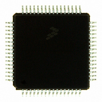
MC9S08AW48CFDE Freescale Semiconductor, MC9S08AW48CFDE Datasheet - Page 249

MC9S08AW48CFDE
Manufacturer Part Number
MC9S08AW48CFDE
Description
IC MCU 48K FLASH 48-QFN
Manufacturer
Freescale Semiconductor
Series
HCS08r
Specifications of MC9S08AW48CFDE
Core Processor
HCS08
Core Size
8-Bit
Speed
40MHz
Connectivity
I²C, SCI, SPI
Peripherals
LVD, POR, PWM, WDT
Number Of I /o
38
Program Memory Size
48KB (48K x 8)
Program Memory Type
FLASH
Ram Size
2K x 8
Voltage - Supply (vcc/vdd)
2.7 V ~ 5.5 V
Data Converters
A/D 8x10b
Oscillator Type
Internal
Operating Temperature
-40°C ~ 85°C
Package / Case
48-QFN
Processor Series
S08AW
Core
HCS08
Data Bus Width
8 bit
Data Ram Size
2 KB
Interface Type
I2C/SCI/SPI
Maximum Clock Frequency
40 MHz
Number Of Programmable I/os
38
Number Of Timers
6
Operating Supply Voltage
- 0.3 V to + 5.8 V
Maximum Operating Temperature
+ 85 C
Mounting Style
SMD/SMT
3rd Party Development Tools
EWS08
Development Tools By Supplier
DEMO9S08AW60E
Minimum Operating Temperature
- 40 C
On-chip Adc
8-ch x 10-bit
Package
48QFN EP
Family Name
HCS08
Maximum Speed
40 MHz
Lead Free Status / RoHS Status
Lead free / RoHS Compliant
Eeprom Size
-
Lead Free Status / Rohs Status
Lead free / RoHS Compliant
- Current page: 249 of 336
- Download datasheet (7Mb)
14.3.1
The ADC analog portion uses V
internally to V
External filtering may be necessary to ensure clean V
14.3.2
The ADC analog portion uses V
internally to V
14.3.3
V
V
driven by an external source that is between the minimum V
must never exceed V
14.3.4
V
V
14.3.5
The ADC module supports up to 28 separate analog inputs. An input is selected for conversion through
the ADCH channel select bits.
14.4
These memory mapped registers control and monitor operation of the ADC:
14.4.1
This section describes the function of the ADC status and control register (ADC1SC1). Writing ADC1SC1
aborts the current conversion and initiates a new conversion (if the ADCH bits are equal to a value other
than all 1s).
Freescale Semiconductor
REFH
DDAD
REFL
SSAD
•
•
•
•
•
•
. If externally available, connect the V
is the low reference voltage for the converter. In some packages, V
is the high reference voltage for the converter. In some packages, V
Status and control register, ADC1SC1
Status and control register, ADC1SC2
Data result registers, ADC1RH and ADC1RL
Compare value registers, ADC1CVH and ADC1CVL
Configuration register, ADC1CFG
Pin enable registers, APCTL1, APCTL2, APCTL3
. If externally available, V
Register Definition
Analog Power (V
Analog Ground (V
Voltage Reference High (V
Voltage Reference Low (V
Analog Channel Inputs (ADx)
Status and Control Register 1 (ADC1SC1)
DD
SS
. If externally available, connect the V
. If externally available, connect the V
DDAD
).
DDAD
SSAD
REFH
DDAD
MC9S08AC16 Series Data Sheet, Rev. 8
SSAD
as its ground connection. In some packages, V
as its power connection. In some packages, V
may be connected to the same potential as V
)
)
REFL
REFL
REFH
pin to the same voltage potential as V
DDAD
)
)
SSAD
DDAD
for good results.
DDAD
pin to the same voltage potential as V
pin to the same voltage potential as V
spec and the V
Analog-to-Digital Converter (S08ADC10V1)
REFL
REFH
is connected internally to
is connected internally to
DDAD
DDAD
DDAD
SSAD
potential (V
SSAD
, or may be
is connected
is connected
.
SS
REFH
DD
.
249
.
Related parts for MC9S08AW48CFDE
Image
Part Number
Description
Manufacturer
Datasheet
Request
R
Part Number:
Description:
Manufacturer:
Freescale Semiconductor, Inc
Datasheet:
Part Number:
Description:
Manufacturer:
Freescale Semiconductor, Inc
Datasheet:
Part Number:
Description:
Manufacturer:
Freescale Semiconductor, Inc
Datasheet:
Part Number:
Description:
Manufacturer:
Freescale Semiconductor, Inc
Datasheet:
Part Number:
Description:
Manufacturer:
Freescale Semiconductor, Inc
Datasheet:
Part Number:
Description:
Manufacturer:
Freescale Semiconductor, Inc
Datasheet:
Part Number:
Description:
Manufacturer:
Freescale Semiconductor, Inc
Datasheet:
Part Number:
Description:
Manufacturer:
Freescale Semiconductor, Inc
Datasheet:
Part Number:
Description:
Manufacturer:
Freescale Semiconductor, Inc
Datasheet:
Part Number:
Description:
Manufacturer:
Freescale Semiconductor, Inc
Datasheet:
Part Number:
Description:
Manufacturer:
Freescale Semiconductor, Inc
Datasheet:
Part Number:
Description:
Manufacturer:
Freescale Semiconductor, Inc
Datasheet:
Part Number:
Description:
Manufacturer:
Freescale Semiconductor, Inc
Datasheet:
Part Number:
Description:
Manufacturer:
Freescale Semiconductor, Inc
Datasheet:
Part Number:
Description:
Manufacturer:
Freescale Semiconductor, Inc
Datasheet:


