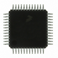
MC9S08DZ60ACLF Freescale Semiconductor, MC9S08DZ60ACLF Datasheet - Page 382

MC9S08DZ60ACLF
Manufacturer Part Number
MC9S08DZ60ACLF
Description
IC MCU 60K FLASH 4K RAM 48-LQFP
Manufacturer
Freescale Semiconductor
Series
HCS08r
Datasheets
1.DEMO9S08DZ60.pdf
(416 pages)
2.EVB9S08DZ60.pdf
(4 pages)
3.MC9S08DZ48AMLF.pdf
(458 pages)
Specifications of MC9S08DZ60ACLF
Core Processor
HCS08
Core Size
8-Bit
Speed
40MHz
Connectivity
CAN, I²C, LIN, SCI, SPI
Peripherals
LVD, POR, PWM, WDT
Number Of I /o
39
Program Memory Size
60KB (60K x 8)
Program Memory Type
FLASH
Eeprom Size
2K x 8
Ram Size
4K x 8
Voltage - Supply (vcc/vdd)
2.7 V ~ 5.5 V
Data Converters
A/D 16x12b
Oscillator Type
External
Operating Temperature
-40°C ~ 85°C
Package / Case
48-LQFP
Processor Series
S08DZ
Core
HCS08
Data Bus Width
8 bit
Data Ram Size
4 KB
Interface Type
CAN, I2C, SCI, SPI
Maximum Clock Frequency
40 MHz
Number Of Programmable I/os
53
Number Of Timers
2
Operating Supply Voltage
5.5 V
Maximum Operating Temperature
+ 85 C
Mounting Style
SMD/SMT
3rd Party Development Tools
EWS08
Development Tools By Supplier
DEMO9S08DZ60
Minimum Operating Temperature
- 40 C
On-chip Adc
12 bit, 24 Channel
For Use With
DEMO9S08DZ60 - BOARD DEMOEVB9S08DZ60 - BOARD EVAL FOR 9S08DZ60
Lead Free Status / RoHS Status
Lead free / RoHS Compliant
Available stocks
Company
Part Number
Manufacturer
Quantity
Price
Company:
Part Number:
MC9S08DZ60ACLF
Manufacturer:
FREESCAL
Quantity:
1 250
Company:
Part Number:
MC9S08DZ60ACLF
Manufacturer:
Freescale Semiconductor
Quantity:
10 000
- Current page: 382 of 458
- Download datasheet (5Mb)
Chapter 17 Development Support
when this timeout occurs is aborted without affecting the memory or operating mode of the target MCU
system.
The custom serial protocol requires the debug pod to know the target BDC communication clock speed.
The clock switch (CLKSW) control bit in the BDC status and control register allows the user to select the
BDC clock source. The BDC clock source can either be the bus or the alternate BDC clock source.
The BKGD pin can receive a high or low level or transmit a high or low level. The following diagrams
show timing for each of these cases. Interface timing is synchronous to clocks in the target BDC, but
asynchronous to the external host. The internal BDC clock signal is shown for reference in counting cycles.
Figure 17-2
The host is asynchronous to the target so there is a 0-to-1 cycle delay from the host-generated falling edge
to where the target perceives the beginning of the bit time. Ten target BDC clock cycles later, the target
senses the bit level on the BKGD pin. Typically, the host actively drives the pseudo-open-drain BKGD pin
during host-to-target transmissions to speed up rising edges. Because the target does not drive the BKGD
pin during the host-to-target transmission period, there is no need to treat the line as an open-drain signal
during this period.
382
SYNCHRONIZATION
PERCEIVED START
(TARGET MCU)
BDC CLOCK
UNCERTAINTY
TRANSMIT 1
TRANSMIT 0
OF BIT TIME
HOST
HOST
shows an external host transmitting a logic 1 or 0 to the BKGD pin of a target HCS08 MCU.
Figure 17-2. BDC Host-to-Target Serial Bit Timing
MC9S08DZ128 Series Data Sheet, Rev. 1
TARGET SENSES BIT LEVEL
10 CYCLES
EARLIEST START
OF NEXT BIT
Freescale Semiconductor
Related parts for MC9S08DZ60ACLF
Image
Part Number
Description
Manufacturer
Datasheet
Request
R
Part Number:
Description:
Manufacturer:
Freescale Semiconductor, Inc
Datasheet:
Part Number:
Description:
Manufacturer:
Freescale Semiconductor, Inc
Datasheet:
Part Number:
Description:
Manufacturer:
Freescale Semiconductor, Inc
Datasheet:
Part Number:
Description:
Manufacturer:
Freescale Semiconductor, Inc
Datasheet:
Part Number:
Description:
Manufacturer:
Freescale Semiconductor, Inc
Datasheet:
Part Number:
Description:
Manufacturer:
Freescale Semiconductor, Inc
Datasheet:
Part Number:
Description:
Manufacturer:
Freescale Semiconductor, Inc
Datasheet:
Part Number:
Description:
Manufacturer:
Freescale Semiconductor, Inc
Datasheet:
Part Number:
Description:
Manufacturer:
Freescale Semiconductor, Inc
Datasheet:
Part Number:
Description:
Manufacturer:
Freescale Semiconductor, Inc
Datasheet:
Part Number:
Description:
Manufacturer:
Freescale Semiconductor, Inc
Datasheet:
Part Number:
Description:
Manufacturer:
Freescale Semiconductor, Inc
Datasheet:
Part Number:
Description:
Manufacturer:
Freescale Semiconductor, Inc
Datasheet:
Part Number:
Description:
Manufacturer:
Freescale Semiconductor, Inc
Datasheet:
Part Number:
Description:
Manufacturer:
Freescale Semiconductor, Inc
Datasheet:


