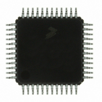
MC9S08DZ60ACLF Freescale Semiconductor, MC9S08DZ60ACLF Datasheet - Page 394

MC9S08DZ60ACLF
Manufacturer Part Number
MC9S08DZ60ACLF
Description
IC MCU 60K FLASH 4K RAM 48-LQFP
Manufacturer
Freescale Semiconductor
Series
HCS08r
Datasheets
1.DEMO9S08DZ60.pdf
(416 pages)
2.EVB9S08DZ60.pdf
(4 pages)
3.MC9S08DZ48AMLF.pdf
(458 pages)
Specifications of MC9S08DZ60ACLF
Core Processor
HCS08
Core Size
8-Bit
Speed
40MHz
Connectivity
CAN, I²C, LIN, SCI, SPI
Peripherals
LVD, POR, PWM, WDT
Number Of I /o
39
Program Memory Size
60KB (60K x 8)
Program Memory Type
FLASH
Eeprom Size
2K x 8
Ram Size
4K x 8
Voltage - Supply (vcc/vdd)
2.7 V ~ 5.5 V
Data Converters
A/D 16x12b
Oscillator Type
External
Operating Temperature
-40°C ~ 85°C
Package / Case
48-LQFP
Processor Series
S08DZ
Core
HCS08
Data Bus Width
8 bit
Data Ram Size
4 KB
Interface Type
CAN, I2C, SCI, SPI
Maximum Clock Frequency
40 MHz
Number Of Programmable I/os
53
Number Of Timers
2
Operating Supply Voltage
5.5 V
Maximum Operating Temperature
+ 85 C
Mounting Style
SMD/SMT
3rd Party Development Tools
EWS08
Development Tools By Supplier
DEMO9S08DZ60
Minimum Operating Temperature
- 40 C
On-chip Adc
12 bit, 24 Channel
For Use With
DEMO9S08DZ60 - BOARD DEMOEVB9S08DZ60 - BOARD EVAL FOR 9S08DZ60
Lead Free Status / RoHS Status
Lead free / RoHS Compliant
Available stocks
Company
Part Number
Manufacturer
Quantity
Price
Company:
Part Number:
MC9S08DZ60ACLF
Manufacturer:
FREESCAL
Quantity:
1 250
Company:
Part Number:
MC9S08DZ60ACLF
Manufacturer:
Freescale Semiconductor
Quantity:
10 000
- Current page: 394 of 458
- Download datasheet (5Mb)
Chapter 18 Debug Module (S08DBGV3) (128K)
18.1.2
The on-chip ICE system can be enabled in all MCU functional modes. The DBG module is disabled if the
MCU is secure. The DBG module comparators are disabled when executing a Background Debug Mode
(BDM) command.
18.1.3
18.2
The DBG module contains no external signals.
394
Figure 18-1
•
Instr. Lastcycle
1. In 64K versions of this module there are only 16 address lines [15:0], there are no core_cpu_aob_14_t2,
core_cpu_aob_15_t2, core_ppage_t2[2:0], and ppage_sel signals.
Ability to End-trace until reset and Begin-trace from reset
Bus Clk
Signal Description
core_cof[1:0]
core_cpu_aob_15_t2
core_ppage_t2[2:0]
Address Bus[16:0]
MCU in BDM
MCU reset
Write Data Bus
Read Data Bus
mmu_ppage_sel
core_cpu_aob_14_t2
DBG Module Enable
Read/Write
Modes of Operation
Block Diagram
shows the structure of the DBG module.
Write Data Bus
Read Data Bus
DBG Read Data Bus
subtract 2
register
Read/Write
1
1
1
1
1
m
u
x
Change of Flow Indicators
MC9S08DZ128 Series Data Sheet, Rev. 1
c
o
n
t
r
o
l
Figure 18-1. DBG Block Diagram
m
u
x
Address/Data/Control Registers
Comparator C
Comparator A
Comparator B
m
u
x
8 deep
FIFO
event only
FIFO Data
control
addr[16:0]
match_A
ppage_sel
match_C
match_B
store
1
1
m
u
x
Trigger
Break
Control
Logic
Freescale Semiconductor
FIFO Data
Read DBGFL
Read DBGFH
Read DBGFX
Tag
Force
Related parts for MC9S08DZ60ACLF
Image
Part Number
Description
Manufacturer
Datasheet
Request
R
Part Number:
Description:
Manufacturer:
Freescale Semiconductor, Inc
Datasheet:
Part Number:
Description:
Manufacturer:
Freescale Semiconductor, Inc
Datasheet:
Part Number:
Description:
Manufacturer:
Freescale Semiconductor, Inc
Datasheet:
Part Number:
Description:
Manufacturer:
Freescale Semiconductor, Inc
Datasheet:
Part Number:
Description:
Manufacturer:
Freescale Semiconductor, Inc
Datasheet:
Part Number:
Description:
Manufacturer:
Freescale Semiconductor, Inc
Datasheet:
Part Number:
Description:
Manufacturer:
Freescale Semiconductor, Inc
Datasheet:
Part Number:
Description:
Manufacturer:
Freescale Semiconductor, Inc
Datasheet:
Part Number:
Description:
Manufacturer:
Freescale Semiconductor, Inc
Datasheet:
Part Number:
Description:
Manufacturer:
Freescale Semiconductor, Inc
Datasheet:
Part Number:
Description:
Manufacturer:
Freescale Semiconductor, Inc
Datasheet:
Part Number:
Description:
Manufacturer:
Freescale Semiconductor, Inc
Datasheet:
Part Number:
Description:
Manufacturer:
Freescale Semiconductor, Inc
Datasheet:
Part Number:
Description:
Manufacturer:
Freescale Semiconductor, Inc
Datasheet:
Part Number:
Description:
Manufacturer:
Freescale Semiconductor, Inc
Datasheet:


