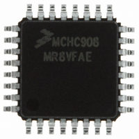
MCHC908MR8VFAE Freescale Semiconductor, MCHC908MR8VFAE Datasheet - Page 134

MCHC908MR8VFAE
Manufacturer Part Number
MCHC908MR8VFAE
Description
IC MCU 8K FLASH 8MHZ PWM 32-LQFP
Manufacturer
Freescale Semiconductor
Series
HC08r
Datasheet
1.MCHC908MR8VFAE.pdf
(372 pages)
Specifications of MCHC908MR8VFAE
Core Processor
HC08
Core Size
8-Bit
Speed
8MHz
Connectivity
SCI
Peripherals
LVD, POR, PWM
Number Of I /o
16
Program Memory Size
8KB (8K x 8)
Program Memory Type
FLASH
Ram Size
256 x 8
Voltage - Supply (vcc/vdd)
4.5 V ~ 5.5 V
Data Converters
A/D 7x10b
Oscillator Type
Internal
Operating Temperature
-40°C ~ 105°C
Package / Case
32-LQFP
Processor Series
HC08MR
Core
HC08
Data Bus Width
8 bit
Data Ram Size
512 B
Interface Type
SCI, SPI
Maximum Clock Frequency
8 MHz
Number Of Programmable I/os
33
Number Of Timers
4
Maximum Operating Temperature
+ 105 C
Mounting Style
SMD/SMT
Development Tools By Supplier
FSICEBASE, M68CBL05CE
Minimum Operating Temperature
- 40 C
On-chip Adc
8 bit, 8 Channel
Lead Free Status / RoHS Status
Lead free / RoHS Compliant
Eeprom Size
-
Lead Free Status / Rohs Status
Details
Available stocks
Company
Part Number
Manufacturer
Quantity
Price
Company:
Part Number:
MCHC908MR8VFAE
Manufacturer:
Freescale
Quantity:
8 393
Company:
Part Number:
MCHC908MR8VFAE
Manufacturer:
Freescale Semiconductor
Quantity:
10 000
- Current page: 134 of 372
- Download datasheet (4Mb)
Clock Generator Module (CGM)
8.11 Acquisition/Lock Time Specifications
8.11.1 Acquisition/Lock Time Definitions
Technical Data
134
To protect the PLLF bit during the break state, write a logic 0 to the
BCFE bit. With BCFE at logic 0 (its default state), software can read and
write the PLL control register during the break state without affecting the
PLLF bit.
The acquisition and lock times of the PLL are, in many applications, the
most critical PLL design parameters. Proper design and use of the PLL
ensures the highest stability and lowest acquisition/lock times.
Typical control systems refer to the acquisition time or lock time as the
reaction time, within specified tolerances, of the system to a step input.
In a PLL, the step input occurs when the PLL is turned on or when it
suffers a noise hit. The tolerance is usually specified as a percent of the
step input or when the output settles to the desired value plus or minus
a percent of the frequency change. Therefore, the reaction time is
constant in this definition, regardless of the size of the step input. For
example, consider a system with a 5 percent acquisition time tolerance.
If a command instructs the system to change from 0 Hz to 1 MHz, the
acquisition time is the time taken for the frequency to reach
1 MHz ± 50 kHz. Fifty kHz = 5 percent of the 1-MHz step input. If the
system is operating at 1 MHz and suffers a –100-kHz noise hit, the
acquisition time is the time taken to return from 900 kHz to
1 MHz ± 5 kHz. Five kHz = 5 percent of the 100-kHz step input.
Other systems refer to acquisition and lock times as the time the system
takes to reduce the error between the actual output and the desired
output to within specified tolerances. Therefore, the acquisition or lock
time varies according to the original error in the output. Minor errors may
not even be registered. Typical PLL applications prefer to use this
definition because the system requires the output frequency to be within
a certain tolerance of the desired frequency regardless of the size of the
initial error.
Clock Generator Module (CGM)
MC68HC908MR8 — Rev 4.1
Freescale Semiconductor
Related parts for MCHC908MR8VFAE
Image
Part Number
Description
Manufacturer
Datasheet
Request
R
Part Number:
Description:
Manufacturer:
Freescale Semiconductor, Inc
Datasheet:
Part Number:
Description:
Manufacturer:
Freescale Semiconductor, Inc
Datasheet:
Part Number:
Description:
Manufacturer:
Freescale Semiconductor, Inc
Datasheet:
Part Number:
Description:
Manufacturer:
Freescale Semiconductor, Inc
Datasheet:
Part Number:
Description:
Manufacturer:
Freescale Semiconductor, Inc
Datasheet:
Part Number:
Description:
Manufacturer:
Freescale Semiconductor, Inc
Datasheet:
Part Number:
Description:
Manufacturer:
Freescale Semiconductor, Inc
Datasheet:
Part Number:
Description:
Manufacturer:
Freescale Semiconductor, Inc
Datasheet:
Part Number:
Description:
Manufacturer:
Freescale Semiconductor, Inc
Datasheet:
Part Number:
Description:
Manufacturer:
Freescale Semiconductor, Inc
Datasheet:
Part Number:
Description:
Manufacturer:
Freescale Semiconductor, Inc
Datasheet:
Part Number:
Description:
Manufacturer:
Freescale Semiconductor, Inc
Datasheet:
Part Number:
Description:
Manufacturer:
Freescale Semiconductor, Inc
Datasheet:
Part Number:
Description:
Manufacturer:
Freescale Semiconductor, Inc
Datasheet:
Part Number:
Description:
Manufacturer:
Freescale Semiconductor, Inc
Datasheet:


