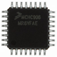
MCHC908MR8VFAE Freescale Semiconductor, MCHC908MR8VFAE Datasheet - Page 307

MCHC908MR8VFAE
Manufacturer Part Number
MCHC908MR8VFAE
Description
IC MCU 8K FLASH 8MHZ PWM 32-LQFP
Manufacturer
Freescale Semiconductor
Series
HC08r
Datasheet
1.MCHC908MR8VFAE.pdf
(372 pages)
Specifications of MCHC908MR8VFAE
Core Processor
HC08
Core Size
8-Bit
Speed
8MHz
Connectivity
SCI
Peripherals
LVD, POR, PWM
Number Of I /o
16
Program Memory Size
8KB (8K x 8)
Program Memory Type
FLASH
Ram Size
256 x 8
Voltage - Supply (vcc/vdd)
4.5 V ~ 5.5 V
Data Converters
A/D 7x10b
Oscillator Type
Internal
Operating Temperature
-40°C ~ 105°C
Package / Case
32-LQFP
Processor Series
HC08MR
Core
HC08
Data Bus Width
8 bit
Data Ram Size
512 B
Interface Type
SCI, SPI
Maximum Clock Frequency
8 MHz
Number Of Programmable I/os
33
Number Of Timers
4
Maximum Operating Temperature
+ 105 C
Mounting Style
SMD/SMT
Development Tools By Supplier
FSICEBASE, M68CBL05CE
Minimum Operating Temperature
- 40 C
On-chip Adc
8 bit, 8 Channel
Lead Free Status / RoHS Status
Lead free / RoHS Compliant
Eeprom Size
-
Lead Free Status / Rohs Status
Details
Available stocks
Company
Part Number
Manufacturer
Quantity
Price
Company:
Part Number:
MCHC908MR8VFAE
Manufacturer:
Freescale
Quantity:
8 393
Company:
Part Number:
MCHC908MR8VFAE
Manufacturer:
Freescale Semiconductor
Quantity:
10 000
- Current page: 307 of 372
- Download datasheet (4Mb)
17.4.1 Polled LVI Operation
17.4.2 Forced Reset Operation
17.4.3 False Reset Protection
MC68HC908MR8 — Rev 4.1
Freescale Semiconductor
$FE0F
Addr.
LVI Status and Control Regis-
Register Name
See page 308.
In applications that can operate at V
monitor V
LVIPWR bit must be at logic 1 to enable the LVI module, and the LVIRST
bit must be at logic 0 to disable LVI resets. TRPSEL in the LVISCR
selects V
In applications that require V
resets allows the LVI module to reset the MCU when V
V
consecutive CPU cycles. In the CONFIG register, the LVIPWR and
LVIRST bits must be at logic 1 to enable the LVI module and to enable
LVI resets. TRPSEL in the LVISCR selects V
The V
supply noise. In order for the LVI module to reset the MCU, V
remain at or below V
must be above V
out of reset. TRPSEL in the LVISCR selects V
(LVISCR)
LVRX
Figure 17-2. LVI I/O Register Summary
DD
ter
level and remains at or below that level for nine or more
LVRX
pin level is digitally filtered to reduce false resets due to power
Read
DD
Write
Re-
set:
by polling the LVIOUT bit. In the configuration register, the
Low-Voltage Inhibit (LVI)
:
:
. See
Bit 7
OUT
LVI-
LVRX
R
R
0
5.4 CONFIG
LVRX
+ V
= Reserved
R
6
0
0
LVHX
for nine or more consecutive CPU cycles. V
DD
TRPS-
for only one CPU cycle to bring the MCU
EL
5
0
to remain above V
Bits.
DD
levels below V
R
4
0
0
LVRX
R
3
0
0
LVRX
.
LVRX
Low-Voltage Inhibit (LVI)
+ V
LVRX
Functional Description
R
2
0
0
DD
LVHX
, enabling LVI
, software can
falls to the
Technical Data
.
R
1
0
0
DD
must
Bit 0
R
0
0
307
DD
Related parts for MCHC908MR8VFAE
Image
Part Number
Description
Manufacturer
Datasheet
Request
R
Part Number:
Description:
Manufacturer:
Freescale Semiconductor, Inc
Datasheet:
Part Number:
Description:
Manufacturer:
Freescale Semiconductor, Inc
Datasheet:
Part Number:
Description:
Manufacturer:
Freescale Semiconductor, Inc
Datasheet:
Part Number:
Description:
Manufacturer:
Freescale Semiconductor, Inc
Datasheet:
Part Number:
Description:
Manufacturer:
Freescale Semiconductor, Inc
Datasheet:
Part Number:
Description:
Manufacturer:
Freescale Semiconductor, Inc
Datasheet:
Part Number:
Description:
Manufacturer:
Freescale Semiconductor, Inc
Datasheet:
Part Number:
Description:
Manufacturer:
Freescale Semiconductor, Inc
Datasheet:
Part Number:
Description:
Manufacturer:
Freescale Semiconductor, Inc
Datasheet:
Part Number:
Description:
Manufacturer:
Freescale Semiconductor, Inc
Datasheet:
Part Number:
Description:
Manufacturer:
Freescale Semiconductor, Inc
Datasheet:
Part Number:
Description:
Manufacturer:
Freescale Semiconductor, Inc
Datasheet:
Part Number:
Description:
Manufacturer:
Freescale Semiconductor, Inc
Datasheet:
Part Number:
Description:
Manufacturer:
Freescale Semiconductor, Inc
Datasheet:
Part Number:
Description:
Manufacturer:
Freescale Semiconductor, Inc
Datasheet:


