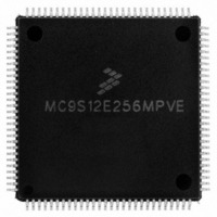
MC9S12E256MPVE Freescale Semiconductor, MC9S12E256MPVE Datasheet - Page 111

MC9S12E256MPVE
Manufacturer Part Number
MC9S12E256MPVE
Description
IC MCU 256K FLASH 25MHZ 112-LQFP
Manufacturer
Freescale Semiconductor
Series
HCS12r
Specifications of MC9S12E256MPVE
Core Processor
HCS12
Core Size
16-Bit
Speed
25MHz
Connectivity
EBI/EMI, I²C, SCI, SPI
Peripherals
POR, PWM, WDT
Number Of I /o
91
Program Memory Size
256KB (256K x 8)
Program Memory Type
FLASH
Ram Size
16K x 8
Voltage - Supply (vcc/vdd)
2.35 V ~ 2.75 V
Data Converters
A/D 16x10b; D/A 2x8b
Oscillator Type
Internal
Operating Temperature
-40°C ~ 125°C
Package / Case
112-LQFP
Processor Series
S12E
Core
HCS12
Data Bus Width
16 bit
Data Ram Size
16 KB
Interface Type
I2C/SCI/SPI
Maximum Clock Frequency
50 MHz
Number Of Programmable I/os
92
Number Of Timers
12
Operating Supply Voltage
0 V to 5 V
Maximum Operating Temperature
+ 125 C
Mounting Style
SMD/SMT
3rd Party Development Tools
EWHCS12
Minimum Operating Temperature
- 40 C
On-chip Adc
16-ch x 10-bit
On-chip Dac
2-ch x 8-bit
For Use With
M68EVB912E128 - BOARD EVAL FOR MC9S12E128/64
Lead Free Status / RoHS Status
Lead free / RoHS Compliant
Eeprom Size
-
Lead Free Status / Rohs Status
Lead free / RoHS Compliant
Available stocks
Company
Part Number
Manufacturer
Quantity
Price
Company:
Part Number:
MC9S12E256MPVE
Manufacturer:
Freescale Semiconductor
Quantity:
10 000
- Current page: 111 of 602
- Download datasheet (4Mb)
2.4.1.3.5
The mass erase command is used to erase a Flash memory block using an embedded algorithm. If the Flash
block to be erased contains any protected area, the PVIOL flag in the FSTAT register will set and the mass
erase command will not launch. After the mass erase command has successfully launched, the CCIF flag
in the FSTAT register will set after the mass erase operation has completed unless a second command has
been buffered.
Freescale Semiconductor
Clock Register
Loaded
Check
Mass Erase Command
Protection
Violation Check
Access
Error Check
Address, Data,
Command
Buffer Empty Check
Bit Polling for
Command
Completion Check
Read: Register FCLKDIV
1.
2.
3.
Bit FDIVLD set?
Figure 2-27. Example Mass Erase Command Flow
yes
Write: Flash Block Address
and Dummy Data
Write: Register FCMD
Mass Erase Command 0x41
Write: Register FSTAT
Clear bit CBEIF 0x80
Read: Register FSTAT
no
no
no
MC9S12E256 Data Sheet, Rev. 1.08
ACCERR
yes
PVIOL
CBEIF
Set?
Set?
Set?
EXIT
Write: Register FCLKDIV
CCIF
Bit
Set?
Bit
Bit
Bit
no
yes
yes
yes
no
Write: Register FSTAT
Clear bit PVIOL 0x20
Clear bit ACCERR 0x10
Write: Register FSTAT
NOTE: command write sequence
aborted by writing 0x00 to
FSTAT register.
NOTE: command write sequence
aborted by writing 0x00 to
FSTAT register.
Read: Register FSTAT
Chapter 2 256 Kbyte Flash Module (FTS256K2V1)
Next Write?
yes
no
111
Related parts for MC9S12E256MPVE
Image
Part Number
Description
Manufacturer
Datasheet
Request
R
Part Number:
Description:
Manufacturer:
Freescale Semiconductor, Inc
Datasheet:
Part Number:
Description:
Manufacturer:
Freescale Semiconductor, Inc
Datasheet:
Part Number:
Description:
Manufacturer:
Freescale Semiconductor, Inc
Datasheet:
Part Number:
Description:
Manufacturer:
Freescale Semiconductor, Inc
Datasheet:
Part Number:
Description:
Manufacturer:
Freescale Semiconductor, Inc
Datasheet:
Part Number:
Description:
Manufacturer:
Freescale Semiconductor, Inc
Datasheet:
Part Number:
Description:
Manufacturer:
Freescale Semiconductor, Inc
Datasheet:
Part Number:
Description:
Manufacturer:
Freescale Semiconductor, Inc
Datasheet:
Part Number:
Description:
Manufacturer:
Freescale Semiconductor, Inc
Datasheet:
Part Number:
Description:
Manufacturer:
Freescale Semiconductor, Inc
Datasheet:
Part Number:
Description:
Manufacturer:
Freescale Semiconductor, Inc
Datasheet:
Part Number:
Description:
Manufacturer:
Freescale Semiconductor, Inc
Datasheet:
Part Number:
Description:
Manufacturer:
Freescale Semiconductor, Inc
Datasheet:
Part Number:
Description:
Manufacturer:
Freescale Semiconductor, Inc
Datasheet:
Part Number:
Description:
Manufacturer:
Freescale Semiconductor, Inc
Datasheet:


