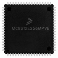
MC9S12E256MPVE Freescale Semiconductor, MC9S12E256MPVE Datasheet - Page 99

MC9S12E256MPVE
Manufacturer Part Number
MC9S12E256MPVE
Description
IC MCU 256K FLASH 25MHZ 112-LQFP
Manufacturer
Freescale Semiconductor
Series
HCS12r
Specifications of MC9S12E256MPVE
Core Processor
HCS12
Core Size
16-Bit
Speed
25MHz
Connectivity
EBI/EMI, I²C, SCI, SPI
Peripherals
POR, PWM, WDT
Number Of I /o
91
Program Memory Size
256KB (256K x 8)
Program Memory Type
FLASH
Ram Size
16K x 8
Voltage - Supply (vcc/vdd)
2.35 V ~ 2.75 V
Data Converters
A/D 16x10b; D/A 2x8b
Oscillator Type
Internal
Operating Temperature
-40°C ~ 125°C
Package / Case
112-LQFP
Processor Series
S12E
Core
HCS12
Data Bus Width
16 bit
Data Ram Size
16 KB
Interface Type
I2C/SCI/SPI
Maximum Clock Frequency
50 MHz
Number Of Programmable I/os
92
Number Of Timers
12
Operating Supply Voltage
0 V to 5 V
Maximum Operating Temperature
+ 125 C
Mounting Style
SMD/SMT
3rd Party Development Tools
EWHCS12
Minimum Operating Temperature
- 40 C
On-chip Adc
16-ch x 10-bit
On-chip Dac
2-ch x 8-bit
For Use With
M68EVB912E128 - BOARD EVAL FOR MC9S12E128/64
Lead Free Status / RoHS Status
Lead free / RoHS Compliant
Eeprom Size
-
Lead Free Status / Rohs Status
Lead free / RoHS Compliant
Available stocks
Company
Part Number
Manufacturer
Quantity
Price
Company:
Part Number:
MC9S12E256MPVE
Manufacturer:
Freescale Semiconductor
Quantity:
10 000
- Current page: 99 of 602
- Download datasheet (4Mb)
2.3.2.9
The banked FCTL register is the Flash control register.
All bits in the FCTL register are readable but are not writable.
The FCTL register is loaded from the Flash Configuration Field byte at $FF0E during the reset sequence,
indicated by F in
2.3.2.10
The banked FADDRHI and FADDRLO registers are the Flash address registers.
All FADDRHI and FADDRLO bits are readable but are not writable. After an array write as part of a
command write sequence, the FADDR registers will contain the mapped MCU address written.
Freescale Semiconductor
NV[7:0]
Reset
Reset
Reset
Field
7-0
W
W
W
R
R
R
NV7
Nonvolatile Bits — The NV[7:0] bits are available as nonvolatile bits. Refer to the Device User Guide for proper
use of the NV bits.
Flash Control Register (FCTL)
Flash Address Registers (FADDR)
F
7
7
0
7
0
Figure
= Unimplemented or Reserved
= Unimplemented or Reserved
= Unimplemented or Reserved
2-13.
NV6
6
F
6
0
6
0
Figure 2-15. Flash Address Low Register (FADDRLO)
Figure 2-14. Flash Address High Register (FADDRHI)
Figure 2-13. Flash Control Register (FCTL)
Table 2-19. FCTL Field Descriptions
NV5
MC9S12E256 Data Sheet, Rev. 1.08
5
F
5
0
5
0
NV4
F
4
4
0
4
0
FADDRLO
FADDRHI
Description
NV3
F
3
3
0
3
0
Chapter 2 256 Kbyte Flash Module (FTS256K2V1)
NV2
2
F
2
0
2
0
NV1
1
F
1
0
1
0
NV0
0
F
0
0
0
0
99
Related parts for MC9S12E256MPVE
Image
Part Number
Description
Manufacturer
Datasheet
Request
R
Part Number:
Description:
Manufacturer:
Freescale Semiconductor, Inc
Datasheet:
Part Number:
Description:
Manufacturer:
Freescale Semiconductor, Inc
Datasheet:
Part Number:
Description:
Manufacturer:
Freescale Semiconductor, Inc
Datasheet:
Part Number:
Description:
Manufacturer:
Freescale Semiconductor, Inc
Datasheet:
Part Number:
Description:
Manufacturer:
Freescale Semiconductor, Inc
Datasheet:
Part Number:
Description:
Manufacturer:
Freescale Semiconductor, Inc
Datasheet:
Part Number:
Description:
Manufacturer:
Freescale Semiconductor, Inc
Datasheet:
Part Number:
Description:
Manufacturer:
Freescale Semiconductor, Inc
Datasheet:
Part Number:
Description:
Manufacturer:
Freescale Semiconductor, Inc
Datasheet:
Part Number:
Description:
Manufacturer:
Freescale Semiconductor, Inc
Datasheet:
Part Number:
Description:
Manufacturer:
Freescale Semiconductor, Inc
Datasheet:
Part Number:
Description:
Manufacturer:
Freescale Semiconductor, Inc
Datasheet:
Part Number:
Description:
Manufacturer:
Freescale Semiconductor, Inc
Datasheet:
Part Number:
Description:
Manufacturer:
Freescale Semiconductor, Inc
Datasheet:
Part Number:
Description:
Manufacturer:
Freescale Semiconductor, Inc
Datasheet:


