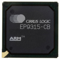
EP9315-CB Cirrus Logic Inc, EP9315-CB Datasheet - Page 192

EP9315-CB
Manufacturer Part Number
EP9315-CB
Description
IC ARM920T MCU 200MHZ 352-PBGA
Manufacturer
Cirrus Logic Inc
Series
EP9r
Specifications of EP9315-CB
Core Processor
ARM9
Core Size
16/32-Bit
Speed
200MHz
Connectivity
EBI/EMI, EIDE, Ethernet, I²C, IrDA, Keypad/Touchscreen, PCMCIA, SPI, UART/USART, USB
Peripherals
AC'97, DMA, I²:S, LCD, LED, MaverickKey, POR, PWM, WDT
Number Of I /o
16
Program Memory Type
ROMless
Ram Size
32K x 8
Voltage - Supply (vcc/vdd)
1.65 V ~ 3.6 V
Data Converters
A/D 8x12b
Oscillator Type
External
Operating Temperature
0°C ~ 70°C
Package / Case
352-BGA
Processor Series
EP93xx
Core
ARM920T
Data Bus Width
32 bit
3rd Party Development Tools
MDK-ARM, RL-ARM, ULINK2
Development Tools By Supplier
EDB9315A-Z
For Use With
598-1144 - KIT DEVELOPMENT EP9315 ARM9
Lead Free Status / RoHS Status
Contains lead / RoHS non-compliant
Eeprom Size
-
Program Memory Size
-
Lead Free Status / Rohs Status
No
Other names
598-1261
Available stocks
Company
Part Number
Manufacturer
Quantity
Price
Part Number:
EP9315-CBZ
Manufacturer:
CIRRUS
Quantity:
20 000
- Current page: 192 of 824
- Download datasheet (13Mb)
7
7-10
Raster Engine With Analog/LCD Integrated Timing and Interface
EP93xx User’s Guide
7.4.3 Video Pixel MUX
7.4.4 Blink Function
words on both the upper and lower half of the bus. The FIFO has an underflow interrupt
indicator that can be used to determine if the system is providing adequate bandwidth and
low enough latency to support the selected display pixel depth, resolution, and refresh rate.
The pixel reconstruction circuitry uses multiplexers and pipe-line registers to 'unpack' the
video pixels that are output from the video FIFO. The stored FIFO words are transferred 2 at
a time across a 64-bit bus. The multiplexers select a single pixel to go on the 24-bit output
bus based on the P value that is written to the
controlled by a pixel counter that also increments based on the PixelMode.P value. The
amount and frequency of data read from the FIFO is dependent on the number of bits per
pixel. For example, in 8 bpp configuration (PixelMode.P = 0x2), the 64-bit FIFO output is
changed for every eight pixels. In dual scan mode, selected by writing DSCAN = ‘1’ to the
“PixelMode”
upper-half screen and lower-half screen pixels are unpacked and loaded into the video
stream sequentially.
The Raster Engine provides blinking pixel control circuitry. This circuitry provides a means to
blink pixels at a rate specified by a programmable count of video frames. The number of
video frames for a blink cycle is controlled by the
blink state bit, so all blinking pixels blink at the same programmed frequency. The most
flexible way to blink pixels is to use a look-up-table (LUT). This is done by logically
transforming the address into the look-up-table based on whether the pixel is a blink pixel,
and whether it is currently in the blink state. For example, a red blinking pixel may be set up
to normally address location 0x11 in the look-up-table. When not in the blink state, the color
output from this location would be red. In the blink state, the address could be logically
modified to 0x21. The color stored at the 0x21 location could be green or black or whatever
other color that it is to be used in place of red in the blink state. To define a pixel as blink,
some color information must be sacrificed. For every pixel color, there could be a blinking
version. This would cut the possible number of system colors in half.
For LUT blinking, the address is modified by using a masked AND/OR/XOR function. The
mask is defined in the
ORed, or XORed with the mask is set by writing to the M field in the
The LUT blinking solution is only useful for 4 bpp and 8 bpp modes because the total number
of colors is limited to 256. The extra bit width in 16 bpp and 24 bpp modes is not used.
Therefore, for 16 bpp, and 24 bpp modes, the LUT blink circuitry is usually bypassed (based
on the C field in the
mathematical operations on the pixel data. These operations can be programmed for Blink to
Background, Blink Dimmer, Blink Brighter, or Blink to Offset by writing the appropriate value
to the M field in the
When Blink to Background mode is enabled, the blink circuitry replaces any blinking pixel
with the
“BkgrndOffset”
register, the upper 32 bits and lower 32 bits are read out in parallel and the
“PixelMode”
“PixelMode”
“BlinkMask”
register value. Setting this register to the background screen color in
Copyright 2007 Cirrus Logic
register.
register) and the blink function is performed by logical or
register. Selection of whether the pixel data is ANDed,
“PixelMode”
“BlinkRate”
register. The multiplexers are
register. There is only a single
“PixelMode”
register.
DS785UM1
Related parts for EP9315-CB
Image
Part Number
Description
Manufacturer
Datasheet
Request
R

Part Number:
Description:
IC ARM9 SOC ENH UNIV 352PBGA
Manufacturer:
Cirrus Logic Inc
Datasheet:

Part Number:
Description:
32-Bit Microcontroller IC
Manufacturer:
Cirrus Logic Inc
Datasheet:

Part Number:
Description:
IC ARM920T MCU 200MHZ 352-PBGA
Manufacturer:
Cirrus Logic Inc
Datasheet:

Part Number:
Description:
MCU, MPU & DSP Development Tools Eval Bd Uni. ARM9 SOC Processor
Manufacturer:
Cirrus Logic Inc
Datasheet:

Part Number:
Description:
IC ARM920T MCU 166MHZ 208-LQFP
Manufacturer:
Cirrus Logic Inc
Datasheet:

Part Number:
Description:
IC ARM920T MCU 200MHZ 352-PBGA
Manufacturer:
Cirrus Logic Inc
Datasheet:

Part Number:
Description:
IC ARM920T MCU 166MHZ 208-LQFP
Manufacturer:
Cirrus Logic Inc
Datasheet:

Part Number:
Description:
Development Kit
Manufacturer:
Cirrus Logic Inc
Datasheet:

Part Number:
Description:
Development Kit
Manufacturer:
Cirrus Logic Inc
Datasheet:

Part Number:
Description:
High-efficiency PFC + Fluorescent Lamp Driver Reference Design
Manufacturer:
Cirrus Logic Inc
Datasheet:

Part Number:
Description:
Development Kit
Manufacturer:
Cirrus Logic Inc
Datasheet:

Part Number:
Description:
Development Kit
Manufacturer:
Cirrus Logic Inc
Datasheet:

Part Number:
Description:
Development Kit
Manufacturer:
Cirrus Logic Inc
Datasheet:

Part Number:
Description:
Ref Bd For Speakerbar MSA & DSP Products
Manufacturer:
Cirrus Logic Inc


