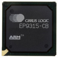
EP9315-CB Cirrus Logic Inc, EP9315-CB Datasheet - Page 245

EP9315-CB
Manufacturer Part Number
EP9315-CB
Description
IC ARM920T MCU 200MHZ 352-PBGA
Manufacturer
Cirrus Logic Inc
Series
EP9r
Specifications of EP9315-CB
Core Processor
ARM9
Core Size
16/32-Bit
Speed
200MHz
Connectivity
EBI/EMI, EIDE, Ethernet, I²C, IrDA, Keypad/Touchscreen, PCMCIA, SPI, UART/USART, USB
Peripherals
AC'97, DMA, I²:S, LCD, LED, MaverickKey, POR, PWM, WDT
Number Of I /o
16
Program Memory Type
ROMless
Ram Size
32K x 8
Voltage - Supply (vcc/vdd)
1.65 V ~ 3.6 V
Data Converters
A/D 8x12b
Oscillator Type
External
Operating Temperature
0°C ~ 70°C
Package / Case
352-BGA
Processor Series
EP93xx
Core
ARM920T
Data Bus Width
32 bit
3rd Party Development Tools
MDK-ARM, RL-ARM, ULINK2
Development Tools By Supplier
EDB9315A-Z
For Use With
598-1144 - KIT DEVELOPMENT EP9315 ARM9
Lead Free Status / RoHS Status
Contains lead / RoHS non-compliant
Eeprom Size
-
Program Memory Size
-
Lead Free Status / Rohs Status
No
Other names
598-1261
Available stocks
Company
Part Number
Manufacturer
Quantity
Price
Part Number:
EP9315-CBZ
Manufacturer:
CIRRUS
Quantity:
20 000
- Current page: 245 of 824
- Download datasheet (13Mb)
Blink Control Registers
BlinkRate
BlinkMask
DS785UM1
31
15
31
15
Address: 0x8003_0040
Default: 0x0000_0000
Definition: Blink Rate Control register
Bit Descriptions:
Address: 0x8003_0044
Default: 0x0000_0000
Definition: Blink Mask register
30
14
30
14
29
13
29
13
28
12
28
12
RSVD:
RATE:
This register is used in conjunction with the
which pixels that are fetched from SDRAM are blink pixels.
RSVD
RSVD
27
11
27
11
26
10
26
10
Copyright 2007 Cirrus Logic
25
25
9
9
Reserved - Unknown during read
Rate - Read/Write
The blink rate value that is written to this field controls the
number of video frames that occur before the LUT
addresses assigned to ‘blink’ change between masked
and unmasked (see
on/off blink cycle is controlled by this equation:
Blink Cycle = 2 x (1/VCLK) x HClkTotal x VLinesTotal x
(255 - BlinkRate)
Raster Engine With Analog/LCD Integrated Timing and Interface
24
24
8
8
MASK
RSVD
23
23
7
7
22
22
6
6
“Blink Function” on page
21
21
5
5
BlinkPattrn
20
20
4
4
MASK
RATE
register to determine
19
19
3
3
EP93xx User’s Guide
18
18
2
2
7-10). The
17
17
1
1
16
16
7-63
0
0
7
Related parts for EP9315-CB
Image
Part Number
Description
Manufacturer
Datasheet
Request
R

Part Number:
Description:
IC ARM9 SOC ENH UNIV 352PBGA
Manufacturer:
Cirrus Logic Inc
Datasheet:

Part Number:
Description:
32-Bit Microcontroller IC
Manufacturer:
Cirrus Logic Inc
Datasheet:

Part Number:
Description:
IC ARM920T MCU 200MHZ 352-PBGA
Manufacturer:
Cirrus Logic Inc
Datasheet:

Part Number:
Description:
MCU, MPU & DSP Development Tools Eval Bd Uni. ARM9 SOC Processor
Manufacturer:
Cirrus Logic Inc
Datasheet:

Part Number:
Description:
IC ARM920T MCU 166MHZ 208-LQFP
Manufacturer:
Cirrus Logic Inc
Datasheet:

Part Number:
Description:
IC ARM920T MCU 200MHZ 352-PBGA
Manufacturer:
Cirrus Logic Inc
Datasheet:

Part Number:
Description:
IC ARM920T MCU 166MHZ 208-LQFP
Manufacturer:
Cirrus Logic Inc
Datasheet:

Part Number:
Description:
Development Kit
Manufacturer:
Cirrus Logic Inc
Datasheet:

Part Number:
Description:
Development Kit
Manufacturer:
Cirrus Logic Inc
Datasheet:

Part Number:
Description:
High-efficiency PFC + Fluorescent Lamp Driver Reference Design
Manufacturer:
Cirrus Logic Inc
Datasheet:

Part Number:
Description:
Development Kit
Manufacturer:
Cirrus Logic Inc
Datasheet:

Part Number:
Description:
Development Kit
Manufacturer:
Cirrus Logic Inc
Datasheet:

Part Number:
Description:
Development Kit
Manufacturer:
Cirrus Logic Inc
Datasheet:

Part Number:
Description:
Ref Bd For Speakerbar MSA & DSP Products
Manufacturer:
Cirrus Logic Inc


