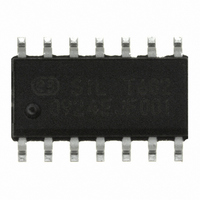
C8051T602-GS Silicon Laboratories Inc, C8051T602-GS Datasheet - Page 106

C8051T602-GS
Manufacturer Part Number
C8051T602-GS
Description
IC 8051 MCU 4K-EEPROM 14-SOIC
Manufacturer
Silicon Laboratories Inc
Series
C8051T60xr
Datasheet
1.C8051T600EDB.pdf
(188 pages)
Specifications of C8051T602-GS
Program Memory Type
OTP
Program Memory Size
4KB (4K x 8)
Package / Case
14-SOIC (3.9mm Width), 14-SOL
Core Processor
8051
Core Size
8-Bit
Speed
25MHz
Connectivity
SMBus (2-Wire/I²C), UART/USART
Peripherals
POR, PWM, Temp Sensor, WDT
Number Of I /o
8
Ram Size
256 x 8
Voltage - Supply (vcc/vdd)
1.8 V ~ 3.6 V
Data Converters
A/D 8x10b
Oscillator Type
Internal
Operating Temperature
-40°C ~ 85°C
Processor Series
C8051T6x
Core
8051
Data Bus Width
8 bit
Data Ram Size
256 B
Interface Type
I2C/SMBus/UART
Maximum Clock Frequency
25 MHz
Number Of Programmable I/os
8
Number Of Timers
3
Maximum Operating Temperature
+ 85 C
Mounting Style
SMD/SMT
3rd Party Development Tools
PK51, CA51, A51, ULINK2
Development Tools By Supplier
C8051T600DK
Minimum Operating Temperature
- 40 C
On-chip Adc
8-ch x 10-bit
Lead Free Status / RoHS Status
Lead free / RoHS Compliant
For Use With
336-1404 - KIT DEV FOR C8051T60X MCU'S
Eeprom Size
-
Lead Free Status / Rohs Status
Lead free / RoHS Compliant
Other names
336-1655-5
Available stocks
Company
Part Number
Manufacturer
Quantity
Price
Company:
Part Number:
C8051T602-GS
Manufacturer:
Silicon Labs
Quantity:
135
C8051T600/1/2/3/4/5/6
22. Port Input/Output
Digital and analog resources are available through eight I/O pins on the C8051T600/1/2/3/4/5, or six I/O
pins on the C8051T606. Port pins P0.0-P0.7 can be defined as general-purpose I/O (GPIO), assigned to
one of the internal digital resources, or assigned to an analog function as shown in Figure 22.1. Port pin
P0.7 is shared with the C2 Interface Data signal (C2D). The designer has complete control over which
functions are assigned, limited only by the number of physical I/O pins. This resource assignment flexibility
is achieved through the use of a Priority Crossbar Decoder. Note that the state of a Port I/O pin can always
be read in the P0 port latch, regardless of the crossbar settings.
The crossbar assigns the selected internal digital resources to the I/O pins based on the Priority Decoder
(Figure 22.3 and Figure 22.4). The registers XBR1 and XBR2, defined in SFR Definition 22.2 and SFR
Definition 22.3, are used to select internal digital functions.
All Port I/Os are 5 V tolerant (refer to Figure 22.2 for the Port cell circuit). The Port I/O cells are configured
as either push-pull or open-drain in the Port Output Mode registers (P0MDOUT). Complete Electrical
Specifications for Port I/O are given in Section “8. Electrical Characteristics” on page 30.
106
Highest
Priority
Lowest
Priority
SYSCLK
Outputs
SMBus
T0, T1
UART
PCA
CP0
Figure 22.1. Port I/O Functional Block Diagram
Port Latch
2
2
2
4
2
P0
(P0.0-P0.7)
8
Rev. 1.2
XBR2 Registers
XBR0, XBR1,
Crossbar
Decoder
Priority
Digital
(ADC0, CP0, VREF, EXTCLK)
To Analog Peripherals
8
P0MDIN Registers
P0MDOUT,
Cells
I/O
P0
P0.0
(‘T600/1/2/3/4/5 Only)
P0.1
P0.2
P0.3
P0.4
P0.5
P0.6
(‘T600/1/2/3/4/5 Only)
P0.7


