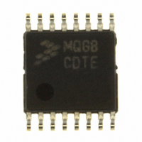
MC9S08QG84CDTE Freescale Semiconductor, MC9S08QG84CDTE Datasheet - Page 123

MC9S08QG84CDTE
Manufacturer Part Number
MC9S08QG84CDTE
Description
IC MCU 8BIT 8K FLASH 16-TSSOP
Manufacturer
Freescale Semiconductor
Series
HCS08r
Datasheet
1.MC9S08QG8CDTER.pdf
(314 pages)
Specifications of MC9S08QG84CDTE
Core Processor
HCS08
Core Size
8-Bit
Speed
20MHz
Connectivity
I²C, SCI, SPI
Peripherals
LVD, POR, PWM, WDT
Number Of I /o
12
Program Memory Size
8KB (8K x 8)
Program Memory Type
FLASH
Ram Size
512 x 8
Voltage - Supply (vcc/vdd)
1.8 V ~ 3.6 V
Data Converters
A/D 8x10b
Oscillator Type
Internal
Operating Temperature
-40°C ~ 85°C
Package / Case
16-TSSOP
Controller Family/series
HCS08
No. Of I/o's
12
Ram Memory Size
512Byte
Cpu Speed
20MHz
No. Of Timers
2
Embedded Interface Type
I2C, SCI, SPI
Rohs Compliant
Yes
For Use With
DEMO9S08QG8E - BOARD DEMO FOR MC9S08QG8
Lead Free Status / RoHS Status
Lead free / RoHS Compliant
Eeprom Size
-
Available stocks
Company
Part Number
Manufacturer
Quantity
Price
Company:
Part Number:
MC9S08QG84CDTE
Manufacturer:
Freescale Semiconductor
Quantity:
135
- Current page: 123 of 314
- Download datasheet (6Mb)
9.2.1
The ADC analog portion uses V
internally to V
External filtering may be necessary to ensure clean V
9.2.2
The ADC analog portion uses V
internally to V
9.2.3
V
V
driven by an external source that is between the minimum V
must never exceed V
9.2.4
V
V
9.2.5
The ADC module supports up to 28 separate analog inputs. An input is selected for conversion through
the ADCH channel select bits.
9.3
These memory mapped registers control and monitor operation of the ADC:
9.3.1
This section describes the function of the ADC status and control register (ADCSC1). Writing ADCSC1
aborts the current conversion and initiates a new conversion (if the ADCH bits are equal to a value other
than all 1s).
Freescale Semiconductor
REFH
DDAD
REFL
SSAD
•
•
•
•
•
•
. If externally available, connect the V
is the low reference voltage for the converter. In some packages, V
is the high reference voltage for the converter. In some packages, V
Status and control register, ADCSC1
Status and control register, ADCSC2
Data result registers, ADCRH and ADCRL
Compare value registers, ADCCVH and ADCCVL
Configuration register, ADCCFG
Pin enable registers, APCTL1, APCTL2, APCTL3
. If externally available, V
Register Definition
Analog Power (V
Analog Ground (V
Voltage Reference High (V
Voltage Reference Low (V
Analog Channel Inputs (ADx)
Status and Control Register 1 (ADCSC1)
DD
SS
. If externally available, connect the V
. If externally available, connect the V
DDAD
).
MC9S08QG8 and MC9S08QG4 Data Sheet, Rev. 5
DDAD
SSAD
REFH
DDAD
SSAD
as its ground connection. In some packages, V
as its power connection. In some packages, V
may be connected to the same potential as V
)
)
REFL
REFL
REFH
pin to the same voltage potential as V
DDAD
)
)
SSAD
DDAD
for good results.
DDAD
pin to the same voltage potential as V
pin to the same voltage potential as V
spec and the V
Analog-to-Digital Converter (S08ADC10V1)
REFL
REFH
is connected internally to
is connected internally to
DDAD
DDAD
DDAD
SSAD
potential (V
SSAD
, or may be
is connected
is connected
.
SS
REFH
DD
.
121
.
Related parts for MC9S08QG84CDTE
Image
Part Number
Description
Manufacturer
Datasheet
Request
R
Part Number:
Description:
Hcs08 Microcontrollers
Manufacturer:
Freescale Semiconductor, Inc
Datasheet:
Part Number:
Description:
Manufacturer:
Freescale Semiconductor, Inc
Datasheet:
Part Number:
Description:
Manufacturer:
Freescale Semiconductor, Inc
Datasheet:
Part Number:
Description:
Manufacturer:
Freescale Semiconductor, Inc
Datasheet:
Part Number:
Description:
Manufacturer:
Freescale Semiconductor, Inc
Datasheet:
Part Number:
Description:
Manufacturer:
Freescale Semiconductor, Inc
Datasheet:
Part Number:
Description:
Manufacturer:
Freescale Semiconductor, Inc
Datasheet:
Part Number:
Description:
Manufacturer:
Freescale Semiconductor, Inc
Datasheet:
Part Number:
Description:
Manufacturer:
Freescale Semiconductor, Inc
Datasheet:
Part Number:
Description:
Manufacturer:
Freescale Semiconductor, Inc
Datasheet:
Part Number:
Description:
Manufacturer:
Freescale Semiconductor, Inc
Datasheet:
Part Number:
Description:
Manufacturer:
Freescale Semiconductor, Inc
Datasheet:
Part Number:
Description:
Manufacturer:
Freescale Semiconductor, Inc
Datasheet:
Part Number:
Description:
Manufacturer:
Freescale Semiconductor, Inc
Datasheet:
Part Number:
Description:
Manufacturer:
Freescale Semiconductor, Inc
Datasheet:


