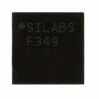
C8051F349-GM Silicon Laboratories Inc, C8051F349-GM Datasheet - Page 231

C8051F349-GM
Manufacturer Part Number
C8051F349-GM
Description
IC 8051 MCU 32K FLASH MEM 32-QFN
Manufacturer
Silicon Laboratories Inc
Series
C8051F34xr
Datasheet
1.C8051F349-GQ.pdf
(276 pages)
Specifications of C8051F349-GM
Program Memory Type
FLASH
Program Memory Size
32KB (32K x 8)
Package / Case
32-QFN
Core Processor
8051
Core Size
8-Bit
Speed
25MHz
Connectivity
SMBus (2-Wire/I²C), SPI, UART/USART, USB
Peripherals
Brown-out Detect/Reset, POR, PWM, WDT
Number Of I /o
25
Ram Size
2.25K x 8
Voltage - Supply (vcc/vdd)
2.7 V ~ 3.6 V
Oscillator Type
Internal
Operating Temperature
-40°C ~ 85°C
Processor Series
C8051F3x
Core
8051
Data Bus Width
8 bit
Data Ram Size
2304 B
Interface Type
I2C, SPI, UART
Maximum Clock Frequency
25 MHz
Number Of Programmable I/os
25
Number Of Timers
4
Operating Supply Voltage
2.7 V to 5.25 V
Maximum Operating Temperature
+ 85 C
Mounting Style
SMD/SMT
3rd Party Development Tools
KSK-SL-F34X, KSK-SL-TOOLSTICK, PK51, CA51, A51, ULINK2
Development Tools By Supplier
C8051F340DK
Minimum Operating Temperature
- 40 C
On-chip Adc
10 bit
Lead Free Status / RoHS Status
Lead free / RoHS Compliant
For Use With
336-1748 - ADAPTER TOOLSTICK FOR C8051F34X
Eeprom Size
-
Data Converters
-
Lead Free Status / Rohs Status
Lead free / RoHS Compliant
Other names
336-1349-5
Available stocks
Company
Part Number
Manufacturer
Quantity
Price
Company:
Part Number:
C8051F349-GM
Manufacturer:
Silicon Labs
Quantity:
135
- Current page: 231 of 276
- Download datasheet (2Mb)
Bits 7–0: SCR7–SCR0: SPI0 Clock Rate.
Example: If SYSCLK = 2 MHz and SPI0CKR = 0x04,
f
Bits 7–0: SPI0DAT: SPI0 Transmit and Receive Data.
SCK
SCR7
f
SCK
R/W
Bit7
R/W
Bit7
=
=
These bits determine the frequency of the SCK output when the SPI0 module is configured
for master mode operation. The SCK clock frequency is a divided version of the system
clock, and is given in the following equation, where SYSCLK is the system clock frequency
and SPI0CKR is the 8-bit value held in the SPI0CKR register.
for 0 <= SPI0CKR <= 255
f
200kHz
SCK
The SPI0DAT register is used to transmit and receive SPI0 data. Writing data to SPI0DAT
places the data into the transmit buffer and initiates a transfer when in Master Mode. A read
of SPI0DAT returns the contents of the receive buffer.
------------------------- -
2
2000000
SCR6
R/W
Bit6
=
R/W
Bit6
4
+
------------------------------------------------ -
2
1
SFR Definition 20.3. SPI0CKR: SPI0 Clock Rate
SPI0CKR
SCR5
SYSCLK
R/W
Bit5
SFR Definition 20.4. SPI0DAT: SPI0 Data
R/W
Bit5
C8051F340/1/2/3/4/5/6/7/8/9/A/B/C/D
SCR4
+
R/W
Bit4
1
R/W
Bit4
SCR3
Rev. 1.3
R/W
Bit3
R/W
Bit3
SCR2
R/W
Bit2
R/W
Bit2
SCR1
R/W
Bit1
R/W
Bit1
SFR Address: 0xA2
SFR Address: 0xA3
SCR0
R/W
Bit0
R/W
Bit0
00000000
Reset Value
00000000
Reset Value
231
Related parts for C8051F349-GM
Image
Part Number
Description
Manufacturer
Datasheet
Request
R
Part Number:
Description:
SMD/C°/SINGLE-ENDED OUTPUT SILICON OSCILLATOR
Manufacturer:
Silicon Laboratories Inc
Part Number:
Description:
Manufacturer:
Silicon Laboratories Inc
Datasheet:
Part Number:
Description:
N/A N/A/SI4010 AES KEYFOB DEMO WITH LCD RX
Manufacturer:
Silicon Laboratories Inc
Datasheet:
Part Number:
Description:
N/A N/A/SI4010 SIMPLIFIED KEY FOB DEMO WITH LED RX
Manufacturer:
Silicon Laboratories Inc
Datasheet:
Part Number:
Description:
N/A/-40 TO 85 OC/EZLINK MODULE; F930/4432 HIGH BAND (REV E/B1)
Manufacturer:
Silicon Laboratories Inc
Part Number:
Description:
EZLink Module; F930/4432 Low Band (rev e/B1)
Manufacturer:
Silicon Laboratories Inc
Part Number:
Description:
I°/4460 10 DBM RADIO TEST CARD 434 MHZ
Manufacturer:
Silicon Laboratories Inc
Part Number:
Description:
I°/4461 14 DBM RADIO TEST CARD 868 MHZ
Manufacturer:
Silicon Laboratories Inc
Part Number:
Description:
I°/4463 20 DBM RFSWITCH RADIO TEST CARD 460 MHZ
Manufacturer:
Silicon Laboratories Inc
Part Number:
Description:
I°/4463 20 DBM RADIO TEST CARD 868 MHZ
Manufacturer:
Silicon Laboratories Inc
Part Number:
Description:
I°/4463 27 DBM RADIO TEST CARD 868 MHZ
Manufacturer:
Silicon Laboratories Inc
Part Number:
Description:
I°/4463 SKYWORKS 30 DBM RADIO TEST CARD 915 MHZ
Manufacturer:
Silicon Laboratories Inc
Part Number:
Description:
N/A N/A/-40 TO 85 OC/4463 RFMD 30 DBM RADIO TEST CARD 915 MHZ
Manufacturer:
Silicon Laboratories Inc
Part Number:
Description:
I°/4463 20 DBM RADIO TEST CARD 169 MHZ
Manufacturer:
Silicon Laboratories Inc


