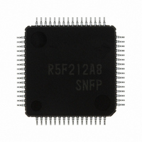
R5F212A8SNFP#U0 Renesas Electronics America, R5F212A8SNFP#U0 Datasheet - Page 102

R5F212A8SNFP#U0
Manufacturer Part Number
R5F212A8SNFP#U0
Description
IC R8C/2A MCU FLASH 64LQFP
Manufacturer
Renesas Electronics America
Series
R8C/2x/2Ar
Specifications of R5F212A8SNFP#U0
Core Processor
R8C
Core Size
16/32-Bit
Speed
20MHz
Connectivity
I²C, LIN, SIO, SSU, UART/USART
Peripherals
POR, PWM, Voltage Detect, WDT
Number Of I /o
55
Program Memory Size
64KB (64K x 8)
Program Memory Type
FLASH
Ram Size
3K x 8
Voltage - Supply (vcc/vdd)
2.2 V ~ 5.5 V
Data Converters
A/D 12x10b; D/A 2x8b
Oscillator Type
Internal
Operating Temperature
-20°C ~ 85°C
Package / Case
64-LQFP
For Use With
R0K5212D8S001BE - KIT STARTER FOR R8C/2DR0K5212D8S000BE - KIT DEV FOR R8C/2D
Lead Free Status / RoHS Status
Lead free / RoHS Compliant
Eeprom Size
-
Available stocks
Company
Part Number
Manufacturer
Quantity
Price
- Current page: 102 of 611
- Download datasheet (7Mb)
R8C/2A Group, R8C/2B Group
Rev.2.00
REJ09B0324-0200
Table 7.32
X: 0 or 1
NOTES:
Table 7.33
X: 0 or 1
NOTES:
Table 7.34
X: 0 or 1
NOTE:
Table 7.35
X: 0 or 1
NOTE:
Register
Setting
Register
Register
Register
Value
Setting
Setting
Setting
1. Pulled up by setting the PU07 bit in the PUR0 register to 1.
2. N-channel open-drain output by setting the CSOS bit in the SSMR2 register to 1 when this pin functions as output.
1. Pulled up by setting the PU07 bit in the PUR0 register to 1.
2. N-channel open-drain output by setting the SCKOS bit in the SSMR2 register to 1 when this pin functions as output.
1. Pulled up by setting the PU07 bit in the PUR0 register to 1.
1. Pulled up by setting the PU07 bit in the PUR0 register to 1.
Value
Value
Value
Bit
Bit
Bit
Bit
Nov 26, 2007
PD3_5
PD3_7
PD3
PD3
PD3_4
X
X
X
0
0
1
1
X
X
X
PD3
PD3_6
0
1
Port P3_4/SDA/SCS
Port P3_5/SCL/SSCK
Port P3_6/(INT1)
Port P3_7/SSO
PD3
X
X
X
0
0
1
1
0
1
0
Clock Synchronous Serial I/O with Chip Select
SSCK output control
Clock Synchronous Serial I/O with Chip Select
(Refer to Table 16.4 Association between
SSO output control
(Refer to Table 16.4 Association between
Communication Modes and I/O Pins .)
Communication Modes and I/O Pins .)
Page 80 of 580
CSS1
X
0
0
0
0
0
1
1
0
0
0
0
0
1
1
X
X
0
0
0
1
1
SSMR2
INT1EN
INTEN
X
X
1
CSS0
X
0
0
0
0
1
0
1
SSCK input control
SSO input control
INT1SEL
IICSEL
PMR
PMR
0
0
0
0
1
0
0
0
X
0
X
0
0
1
X
X
1
X
X
0
0
1
0
0
ICCR1
Input port
Output port
INT1 input
ICE
IICSEL
X
X
X
X
0
0
1
PMR
SSMR2
SOOS
0
X
0
X
0
0
1
X
0
0
0
1
(1)
Input port
Output port
SCS input
SCS output
SDA input/output
ICCR1
ICE
X
X
0
0
0
0
1
IICSEL
PMR
0
1
0
1
0
0
0
Input port
Output port
SSCK input
SSCK output
SCL input/output
(1)
(2)
(2)
Input port
Output port
SSO input
SSO output (CMOS output)
SSO output (N-channel open-drain
output)
Function
(1)
7. Programmable I/O Ports
Function
(2)
(2)
(1)
Function
Function
Related parts for R5F212A8SNFP#U0
Image
Part Number
Description
Manufacturer
Datasheet
Request
R

Part Number:
Description:
KIT STARTER FOR M16C/29
Manufacturer:
Renesas Electronics America
Datasheet:

Part Number:
Description:
KIT STARTER FOR R8C/2D
Manufacturer:
Renesas Electronics America
Datasheet:

Part Number:
Description:
R0K33062P STARTER KIT
Manufacturer:
Renesas Electronics America
Datasheet:

Part Number:
Description:
KIT STARTER FOR R8C/23 E8A
Manufacturer:
Renesas Electronics America
Datasheet:

Part Number:
Description:
KIT STARTER FOR R8C/25
Manufacturer:
Renesas Electronics America
Datasheet:

Part Number:
Description:
KIT STARTER H8S2456 SHARPE DSPLY
Manufacturer:
Renesas Electronics America
Datasheet:

Part Number:
Description:
KIT STARTER FOR R8C38C
Manufacturer:
Renesas Electronics America
Datasheet:

Part Number:
Description:
KIT STARTER FOR R8C35C
Manufacturer:
Renesas Electronics America
Datasheet:

Part Number:
Description:
KIT STARTER FOR R8CL3AC+LCD APPS
Manufacturer:
Renesas Electronics America
Datasheet:

Part Number:
Description:
KIT STARTER FOR RX610
Manufacturer:
Renesas Electronics America
Datasheet:

Part Number:
Description:
KIT STARTER FOR R32C/118
Manufacturer:
Renesas Electronics America
Datasheet:

Part Number:
Description:
KIT DEV RSK-R8C/26-29
Manufacturer:
Renesas Electronics America
Datasheet:

Part Number:
Description:
KIT STARTER FOR SH7124
Manufacturer:
Renesas Electronics America
Datasheet:

Part Number:
Description:
KIT STARTER FOR H8SX/1622
Manufacturer:
Renesas Electronics America
Datasheet:

Part Number:
Description:
KIT DEV FOR SH7203
Manufacturer:
Renesas Electronics America
Datasheet:


