M38869FFAHP#UU Renesas Electronics America, M38869FFAHP#UU Datasheet
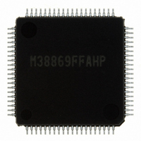
M38869FFAHP#UU
Specifications of M38869FFAHP#UU
Available stocks


Related parts for M38869FFAHP#UU


M38869FFAHP#UU Summary of contents
Page 1
To our customers, Old Company Name in Catalogs and Other Documents st On April 1 , 2010, NEC Electronics Corporation merged with Renesas Technology Corporation, and Renesas Electronics Corporation took over all the business of both companies. Therefore, although the ...
Page 2
All information included in this document is current as of the date this document is issued. Such information, however, is subject to change without any prior notice. Before purchasing or using any Renesas Electronics products listed herein, please confirm ...
Page 3
To all our customers Regarding the change of names mentioned in the document, such as Mitsubishi Electric and Mitsubishi XX, to Renesas Technology Corp. The semiconductor operations of Hitachi and Mitsubishi Electric were transferred to Renesas Technology Corporation on April ...
Page 4
DESCRIPTION The 3886 group is the 8-bit microcomputer based on the 740 fam- ily core technology. The 3886 group is designed for controlling systems that require analog signal processing and include two serial I/O functions, A-D converters, D-A converters, system ...
Page 5
PIN CONFIGURATION (TOP VIEW ...
Page 6
PIN CONFIGURATION (TOP VIEW) P3 /PWM /PWM / / / / / / / ...
Page 7
FUNCTIONAL BLOCK Fig. 4 Functional block diagram 4 MITSUBISHI MICROCOMPUTERS 3886 Group SINGLE-CHIP 8-BIT CMOS MICROCOMPUTER ...
Page 8
PIN DESCRIPTION Table 1 Pin description (1) Pin Name •Apply voltage of 2.7 V – 5 Vcc, and Vss Power source CC SS •In the flash memory version, apply voltage of 4.0 ...
Page 9
Table 2 Pin description (2) Pin Name COUT CIN P4 /INT 2 0 /OBF 00 P4 /INT 3 1 I/O port P4 /OBF 01 P4 /RxD 4 P4 /TxD CLK1 ...
Page 10
PART NUMBERING Fig. 5 Part numbering SINGLE-CHIP 8-BIT CMOS MICROCOMPUTER ...
Page 11
GROUP EXPANSION Mitsubishi plans to expand the 3886 group as follows. Memory Type Support for mask ROM, One Time PROM, EPROM and flash memory version. Memory Size ROM size ........................................................... bytes RAM size .......................................................... 1024 ...
Page 12
FUNCTIONAL DESCRIPTION CENTRAL PROCESSING UNIT (CPU) The 3886 group uses the standard 740 Family instruction set. Re- fer to the table of 740 Family addressing modes and machine instructions or the 740 Family Software Manual for details on the instruction ...
Page 13
MEMORY Special Function Register (SFR) Area The Special Function Register area in the zero page contains con- trol registers such as I/O ports and timers. RAM RAM is used for data storage and for stack area of subroutine calls and ...
Page 14
...
Page 15
I/O PORTS The I/O ports have direction registers which determine the input/ output direction of each individual pin. Each bit in a direction reg- ister corresponds to one pin, and each pin can be set to be input port or ...
Page 16
Table 5 I/O port function (2) Name Pin Input/Output /INT /INT Port P5 P5 /INT /CNTR /CNTR ...
Page 17
– ...
Page 18
...
Page 19
...
Page 20
...
Page 21
Fig. 14 Structure of port I/O related register 18 MITSUBISHI MICROCOMPUTERS SINGLE-CHIP 8-BIT CMOS MICROCOMPUTER ...
Page 22
INTERRUPTS Interrupts occur by 16 sources among 21 sources: nine external, eleven internal, and one software. Interrupt Control Each interrupt is controlled by an interrupt request bit, an interrupt enable bit, and the interrupt disable flag except for the software ...
Page 23
Table 6 Interrupt vector addresses and priority Vector Addresses (Note 1) Interrupt Source Priority High Reset (Note 2) 1 FFFD 16 INT 0 2 FFFB 16 Input buffer full (IBF) INT 1 3 FFF9 16 Output buffer empty (OBE) Serial ...
Page 24
...
Page 25
...
Page 26
Key Input Interrupt (Key-on Wake Up) A Key input interrupt request is generated by applying “L” level to any pin of port P3 that have been set to input mode. In other words generated when AND of input ...
Page 27
TIMERS The 3886 group has four timers: timer X, timer Y, timer 1, and timer 2. The division ratio of each timer or prescaler is given by 1/(n + 1), where n is the value in the corresponding timer or ...
Page 28
...
Page 29
SERIAL I/O Serial I/O1 Serial I/O1 can be used as either clock synchronous or asynchro- nous (UART) serial I/O. A dedicated timer is also provided for baud rate generation ...
Page 30
Asynchronous Serial I/O (UART) Mode Clock asynchronous serial I/O mode (UART) can be selected by clearing the serial I/O1 mode selection bit of the serial I/O1 control register to “0”. Eight serial data transfer formats can be selected, and ...
Page 31
...
Page 32
...
Page 33
Serial I/O2 The serial I/O2 function can be used only for clock synchronous serial I/O. For clock synchronous serial I/O the transmitter and the receiver must use the same clock. If the internal clock is used, transfer is started by ...
Page 34
...
Page 35
PULSE WIDTH MODULATION (PWM) OUTPUT CIRCUIT The 3886 group has two PWM output circuits, PWM0 and PWM1, with 14-bit resolution respectively. These can operate indepen- dently. When the oscillation frequency X minimum resolution bit width is 200 ns and the ...
Page 36
Data Setup (PWM0) The PWM0 output pin also functions as port P3 PWM0 output pin is selected from either P3 P5 /PWM by bit 4 of the AD/DA control register (address 6 01 0034 ). 16 The PWM0 output becomes ...
Page 37
...
Page 38
BUS INTERFACE The 3886 group has a 2-byte bus interface function which is al- most functionally equal to MELPS8-41 series and the control signal from the host CPU side can operate it (slave mode possible to connect the ...
Page 39
Fig. 33 Structure of bus interface related register 36 MITSUBISHI MICROCOMPUTERS SINGLE-CHIP 8-BIT CMOS MICROCOMPUTER ...
Page 40
...
Page 41
Bus Buffer Status Register 0, 1 (DBBSTS0, DBBSTS1)] 0029 16 The data bus buffer status register 0, 1 consist of eight bits. Bits 0, 1, and 3 are read-only bits and indicate the condition of the data bus buffer. ...
Page 42
Table 8 Function description of control I/O pins at bus interface function selected OBF 00 output Pin Name enable bit P4 /SRDY – – /INT 1 20 ...
Page 43
MULTI-MASTER I C-BUS INTERFACE 2 The multi-master I C-BUS interface is a serial communications cir- 2 cuit, conforming to the Philips I C-BUS data transfer format. This interface, offering both arbitration lost detection and a synchro ...
Page 44
C Data Shift Register (S0)] 0012 2 The I C data shift register (S0 : address 0012 register to store receive data and write transmit data. When transmit data is written into this register transferred to ...
Page 45
C Clock Control Register (S2)] 0016 2 The I C clock control register (address 0016 control, S mode and S frequency •Bits frequency control bits (CCR0–CCR4) CL These bits control the S ...
Page 46
C Control Register (S1D)] 0015 2 The I C control register (address 0015 ) controls data communi- 16 cation format. •Bits Bit counter (BC0–BC2) These bits decide the number of bits for the next 1-byte ...
Page 47
C Status Register (S1)] 0014 2 The I C status register (address 0014 ) controls the I 16 terface status. The low-order 4 bits are read-only bits and the high-order 4 bits can be read out and written ...
Page 48
Communication mode specification bit (transfer direc- tion specification bit: TRX) This bit decides a direction of transfer for data communication. When this bit is “0,” the reception mode is selected and the data of a transmitting device is ...
Page 49
START Condition Generating Method When writing “1” to the MST, TRX, and BB bits of the I register (address 0014 ) at the same time after writing the slave 16 2 address to the I C data shift register (address ...
Page 50
C START/STOP Condition Control Register (S2D)] 0017 16 2 The I C START/STOP condition control register (address 0017 controls START/STOP condition detection. •Bits START/STOP condition set bit (SSC4–SSC0) S release time, setup time, and hold ...
Page 51
...
Page 52
Example of Master Transmission An example of master transmission in the standard clock mode, at the S frequency of 100 kHz and in the ACK return mode is CL shown below. Set a slave address in the high-order 7 bits ...
Page 53
START condition generating procedure using multi-master 1. Procedure example (The necessary conditions of the generat- ing procedure are described as the following LDA — (Taking out of slave address value) SEI (Interrupt disabled) BBS 5, S1, ...
Page 54
A-D CONVERTER [A-D Conversion Register 1,2 (AD1, AD2)] 0035 , 0038 16 16 The A-D conversion register is a read-only register that stores the result of an A-D conversion. When reading this register during an A-D conversion, the previous conversion ...
Page 55
...
Page 56
D-A CONVERTER The 3886 group has two internal D-A converters (DA with 8-bit resolution. The D-A converter is performed by setting the value in each D-A conversion register. The result of D-A conversion is output from the ...
Page 57
COMPARATOR CIRCUIT Comparator Configuration The comparator circuit consists of resistors, comparators, a com- parator control circuit, the comparator reference input selection bit (bit 7 of address 001D ), a comparator data register (address 16 002D ), the comparator reference power ...
Page 58
WATCHDOG TIMER The watchdog timer gives a mean of returning to the reset status when a program cannot run on a normal loop (for example, be- cause of a software run-away). The watchdog timer consists of an 8-bit watchdog timer ...
Page 59
RESET CIRCUIT To reset the microcomputer, RESET pin should be held at an "L" level for more. Then the RESET pin is returned to an "H" level (the power source voltage should be between 2.7 V and ...
Page 60
...
Page 61
CLOCK GENERATING CIRCUIT The 3886 group has two built-in oscillation circuits. An oscillation circuit can be formed by connecting a resonator between and X ). Use the circuit constants in accordance OUT CIN COUT with the resonator ...
Page 62
“ 0 ” “ 1 ” ...
Page 63
“ 1 ” ...
Page 64
PROCESSOR MODE Single-chip mode, memory expansion mode, and microprocessor mode in the M38867M8A/E8A can be selected by changing the contents of the processor mode bits (CM and CM 0 address 003B ). In memory expansion mode and microprocessor 16 mode, ...
Page 65
BUS CONTROL AT MEMORY EXPANSION The M38867M8A/E8A have a built-in ONW function to facilitate access to an external (expanded) memory and I/O devices in memory expansion mode or microprocessor mode “L” level signal is input to the P3 ...
Page 66
EPROM MODE The built-in PROM of the blank One Time PROM version and built- in EPROM version can be read or programmed with a general-purpose PROM programmer using a special programming adapter. The One Time PROM version and the built-in ...
Page 67
FLASH MEMORY MODE The M38869FFAHP/GP has the flash memory mode in addition to the normal operation mode (microcomputer mode). The user can use this mode to perform read, program, and erase operations for the internal flash memory. The M38869FFAHP/GP has ...
Page 68
Table 20 Pin description (flash memory parallel I/O mode) Pin Name /Output Power supply CC SS CNV V input SS PP _____ RESET Reset input X Clock input IN X Clock output Output OUT AV Analog supply ...
Page 69
...
Page 70
Read-only Mode The microcomputer enters the read-only mode by applying V to the V pin. In this mode, the user can input the address memory location to be read and the control signals at the timing V ...
Page 71
Read command The microcomputer enters the read mode by inputting command code “00 ” in the first cycle. The command code is latched into 16 the internal command latch at the rising edge of the WE input. When the address ...
Page 72
Program command The microcomputer enters the program mode by inputting com- mand code “40 ” in the first cycle. The command code is latched 16 into the internal command latch at the rising edge of the WE input. When the ...
Page 73
Erase command The erase command is executed by inputting command code 20 in the first cycle and command code 20 16 cycle. The command code is latched into the internal command ___ latch at the rising edges of the WE ...
Page 74
Reset command The reset command provides a means of stopping execution of the erase or program command safely. If the user inputs command code FF in the second cycle after inputting the erase or program 16 command in the first ...
Page 75
Program START ADRS = first location WRITE PROGRAM COMMAND WRITE PROGRAM DATA DURATION = WRITE PROGRAM-VERIFY COMMAND DURATION = 6 ...
Page 76
Table 22 DC ELECTRICAL CHARACTERISTICS (T Symbol Parameter I SB1 V supply current (at standby SB2 I V supply current (at read) CC1 supply current (at program) CC2 supply current (at erase) ...
Page 77
Flash memory mode 2 (serial I/O mode) The M38869FFAHP/GP has a function to serially input/output the software commands, addresses, and data required for operation on the internal flash memory (e. g., read, program, and erase) us- ing only a ...
Page 78
Table 25 Pin description (flash memory serial I/O mode) Pin Name /Output Power supply CC SS CNV V input SS PP _____ RESET Reset input X Clock input IN X Clock output Output OUT AV Analog supply ...
Page 79
Functional Outline (serial I/O mode) In the serial I/O mode, data is transferred synchronously with the clock using serial input/output. The input data is read from the SDA pin into the internal circuit synchronously with the rising edge of the ...
Page 80
Program command Input command code 40 in the first transfer. Proceed and input 16 the low-order 8 bits and the high-order 8 bits of the address and then program data. Programming is initiated at the last rising edge of the ...
Page 81
Erase command Input command code 20 in the first transfer and command code 16 20 again in the second transfer. When this is done, the 16 M38869FFAHP/GP executes an erase command. Erase is initi- ated at the last rising edge ...
Page 82
Error check command Input command code 80 in the first transfer, and the 16 M38869FFAHP/GP outputs error information from the SDA pin, beginning at the next falling edge of the serial clock. If the LSB bit of the 8-bit error ...
Page 83
DC ELECTRICAL CHARACTERISTICS -relevant standards during read, program, and erase are the same as in the parallel input/output mode for the SCLK, SDA, BUSY, OE pins conform to the microcomputer modes. IL ...
Page 84
Flash memory mode 3 (CPU reprogramming mode) The M38869FFAHP/GP has the CPU reprogramming mode where a built-in flash memory is handled by the central processing unit (CPU). In CPU reprogramming mode, the flash memory is handled by writing and ...
Page 85
CPU reprogramming mode operation procedure The operation procedure in CPU reprogramming mode is de- scribed below. < Beginning procedure > Apply the CNVss/V pin for reset release. PP After CPU reprogramming mode control program is transferred to ...
Page 86
Program command When “40 ” is written to the flash command register, the 16 M38869FFAHP/GP enters the program mode. Subsequently to this, if the instruction (for instance, STA instruction) for writing byte data in the address to be programmed is ...
Page 87
Program START ADRS = first location WRITE PROGRAM COMMAND WRITE PROGRAM DATA WAIT ERASE PROGRAM BUSY FLAG = 0 YES WRITE PROGRAM-VERIFY COMMAND DURATION = ...
Page 88
NOTES ON PROGRAMMING Processor Status Register The contents of the processor status register (PS) after a reset are undefined, except for the interrupt disable flag (I) which is “1.” Af- ter a reset, initialize flags which affect program execution. In ...
Page 89
NOTES ON USAGE Handling of Power Source Pins In order to avoid a latch-up occurrence, connect a capacitor suit- able for high frequencies as bypass capacitor between power source pin (V pin) and GND pin ( source pin ...
Page 90
ELECTRICAL CHARACTERISTICS Table 28 Absolute maximum ratings Symbol Parameter V Power source voltage (Note Power source voltage (Note Input voltage P0 – – ...
Page 91
Table 29 Recommended operating conditions (V = 2 4.0 to 5.5 V for flash memory version Symbol V CC Power source voltage (except flash memory version Power source voltage (flash ...
Page 92
Table 30 Recommended operating conditions (V = 2 4.0 to 5.5 V for flash memory version Symbol I “H” total peak output current OH(peak) “H” total peak output current I OH(peak) “L” ...
Page 93
Table 31 Recommended operating conditions (V = 2 4.0 to 5.5 V for flash memory version Symbol “H” peak output current I OH(peak) “L” peak output current I OL(peak) “L” peak output ...
Page 94
Table 32 Electrical characteristics (V = 2 4.0 to 5.5 V for flash memory version Symbol Parameter “H” output voltage P0 – – ...
Page 95
Table 33 Electrical characteristics (V = 2 4.0 to 5.5 V for flash memory version Symbol Parameter I Power source current CC 92 SINGLE-CHIP 8-BIT CMOS MICROCOMPUTER = ...
Page 96
Table 34 A-D converter characteristics ( 2 4.0 to 5.5 V for flash memory version otherwise noted) 10-bit A-D mode (when conversion mode selection bit (bit 7 of address 0038 ...
Page 97
TIMING REQUIREMENTS Table 38 Timing requirements ( 4 – °C, unless otherwise noted Symbol t (RESET) Reset input “L” pulse width ...
Page 98
Table 39 Timing requirements ( 2 – °C, unless otherwise noted Symbol t (RESET) Reset input “L” pulse width Main ...
Page 99
Table 40 Timing requirements for system bus interface (V = 4 – °C, unless otherwise noted Symbol t (S- setup time 0 ...
Page 100
Table 42 Switching characteristics 4 – °C, unless otherwise noted Symbol Serial I/O1 clock output “H” pulse width WH CLK1 ...
Page 101
Table 44 Switching characteristics for system bus interface (V = 4 – °C, unless otherwise noted Symbol t (R-D) After read data output enable time a ...
Page 102
Table 46 Timing requirements in memory expansion mode and microprocessor mode (V = 4 – °C, in high-speed mode, unless otherwise noted Symbol t (ONW- ) ...
Page 103
Fig. 83 Circuit for measuring output switching characteristics (1) 100 ...
Page 104
...
Page 105
...
Page 106
...
Page 107
...
Page 108
Table 48 Multi-master I C-BUS bus line characteristics Symbol t Bus free time BUF t Hold time for START condition HD;STA t Hold time for S clock = “0” LOW CL t Rising time of both S and S ...
Page 109
PACKAGE OUTLINE 80P6Q-A EIAJ Package Code JEDEC Code LQFP80-P-1212-0.5 – 80D0 EIAJ Package Code JEDEC Code – – 21.0 0.2 INDEX 106 SINGLE-CHIP 8-BIT CMOS MICROCOMPUTER ...
Page 110
EIAJ Package Code JEDEC Code QFP80-P-1414-0. SINGLE-CHIP 8-BIT CMOS MICROCOMPUTER Weight(g) Lead Material Alloy 42 1. Detail F ...
Page 111
REVISION DESCRIPTION LIST Rev. No. 1.0 First Edition 2.0 The contents of flash memory version were added. 2.1 All pages; “PRELIMINARY Notice: This is...” eliminated. Page 1; The second “In high-speed mode” of “Power dissipation” eliminated. Page 1; “Memory expansion” ...
Page 112
REVISION DESCRIPTION LIST Rev. No. 2.1 Page 73; Minimum limits of V Page 74; Figure 72 is partly revised. Page 81; Explanation of “Flash memory mode 3 (CPU reprogramming mode)” is added. Page 81; Note into Figure 79 is eliminated ...
Page 113
Keep safety first in your circuit designs! • Mitsubishi Electric Corporation puts the maximum effort into making semiconductor products better and more reliable, but there is always the possibility that trouble may occur with them. Trouble with semiconductors may lead ...