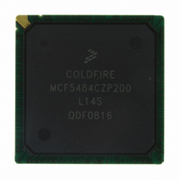
MCF5484CZP200 Freescale Semiconductor, MCF5484CZP200 Datasheet - Page 19

MCF5484CZP200
Manufacturer Part Number
MCF5484CZP200
Description
IC MPU 32BIT COLDF 388-PBGA
Manufacturer
Freescale Semiconductor
Series
MCF548xr
Datasheet
1.MCF5480CVR166.pdf
(34 pages)
Specifications of MCF5484CZP200
Core Processor
Coldfire V4E
Core Size
32-Bit
Speed
200MHz
Connectivity
CAN, EBI/EMI, Ethernet, I²C, SPI, UART/USART, USB
Peripherals
DMA, PWM, WDT
Number Of I /o
99
Program Memory Type
ROMless
Ram Size
32K x 8
Voltage - Supply (vcc/vdd)
1.43 V ~ 1.58 V
Oscillator Type
External
Operating Temperature
-40°C ~ 85°C
Package / Case
388-BGA
Program Memory Size
64KB
Cpu Speed
200MHz
Embedded Interface Type
I2C, UART, DMA
Digital Ic Case Style
BGA
No. Of Pins
388
Supply Voltage Range
3V To 3.6V, 1.43V To 1.58V
Rohs Compliant
No
For Use With
M5485EVBGHSE - KIT DEV GHS FOR M5485EVBM5485EVBGHS - KIT DEV GHS FOR M5485EVBM5485BFEE - MODULE MCF5485 FIRE ENGINEM5485AFEE - MODULE MCF5485 FIRE ENGINEM5485AFE - MODULE MCF5485 FIRE ENGINEM5484GFEE - MODULE M5484 FIRE ENGINEM5484LITEKITE - KIT DEV FOR MCF548X FAMILY
Lead Free Status / RoHS Status
Contains lead / RoHS non-compliant
Eeprom Size
-
Program Memory Size
-
Data Converters
-
Available stocks
Company
Part Number
Manufacturer
Quantity
Price
Company:
Part Number:
MCF5484CZP200
Manufacturer:
Exar
Quantity:
100
Company:
Part Number:
MCF5484CZP200
Manufacturer:
FREESCAL
Quantity:
185
Company:
Part Number:
MCF5484CZP200
Manufacturer:
Freescale Semiconductor
Quantity:
10 000
Freescale Semiconductor
1
2
3
4
5
6
7
8
9
10
11
Symbol
DD13
DD14
DD15
DD16
The frequency of operation is 2x or 4x the CLKIN frequency of operation. The MCF548X supports a single external
reference clock (CLKIN). This signal defines the frequency of operation for FlexBus and PCI, but SDRAM clock operates at
the same frequency as the internal bus clock. Please see the reset configuration signals description in the “Signal
Descriptions” chapter within the MCF548x Reference Manual.
SDCLK is one memory clock in (ns).
Pulse width high plus pulse width low cannot exceed max clock period.
Pulse width high plus pulse width low cannot exceed max clock period.
Command output valid should be 1/2 the memory bus clock (SDCLK) plus some minor adjustments for process,
temperature, and voltage variations.
This specification relates to the required input setup time of today’s DDR memories. SDDATA[31:24] is relative to SDDQS3,
SDDATA[23:16] is relative to SDDQS2, SDDATA[15:8] is relative to SDDQS1, and SDDATA[7:0] is relative SDDQS0.
The first data beat is valid before the first rising edge of SDDQS and after the SDDQS write preamble. The remaining data
beats is valid for each subsequent SDDQS edge.
This specification relates to the required hold time of today’s DDR memories. SDDATA[31:24] is relative to SDDQS3,
SDDATA[23:16] is relative to SDDQS2, SDDATA[15:8] is relative to SDDQS1, and SDDATA[7:0] is relative SDDQS0.
Data input skew is derived from each SDDQS clock edge. It begins with a SDDQS transition and ends when the last data
line becomes valid. This input skew must include DDR memory output skew and system level board skew (due to routing
or other factors).
Data input hold is derived from each SDDQS clock edge. It begins with a SDDQS transition and ends when the first data
line becomes invalid.
DDR memories typically have a minimum speed specification of 83 MHz. Check memory component specifications to verify.
DQS input read preamble width (t
DQS input read postamble width (t
DQS output write preamble width (t
DQS output write postamble width (t
Table 13. DDR Timing Specifications (continued)
Characteristic
MCF548x ColdFire
RPRE
RPST
WPRE
WPST
)
)
)
)
®
Microprocessor, Rev. 4
0.25
Min
0.9
0.4
0.4
Max
1.1
0.6
0.6
—
SDCLK
SDCLK
SDCLK
SDCLK
Unit
SDRAM Bus
Notes
19


