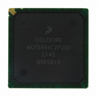
MCF5484CZP200 Freescale Semiconductor, MCF5484CZP200 Datasheet - Page 6

MCF5484CZP200
Manufacturer Part Number
MCF5484CZP200
Description
IC MPU 32BIT COLDF 388-PBGA
Manufacturer
Freescale Semiconductor
Series
MCF548xr
Datasheet
1.MCF5480CVR166.pdf
(34 pages)
Specifications of MCF5484CZP200
Core Processor
Coldfire V4E
Core Size
32-Bit
Speed
200MHz
Connectivity
CAN, EBI/EMI, Ethernet, I²C, SPI, UART/USART, USB
Peripherals
DMA, PWM, WDT
Number Of I /o
99
Program Memory Type
ROMless
Ram Size
32K x 8
Voltage - Supply (vcc/vdd)
1.43 V ~ 1.58 V
Oscillator Type
External
Operating Temperature
-40°C ~ 85°C
Package / Case
388-BGA
Program Memory Size
64KB
Cpu Speed
200MHz
Embedded Interface Type
I2C, UART, DMA
Digital Ic Case Style
BGA
No. Of Pins
388
Supply Voltage Range
3V To 3.6V, 1.43V To 1.58V
Rohs Compliant
No
For Use With
M5485EVBGHSE - KIT DEV GHS FOR M5485EVBM5485EVBGHS - KIT DEV GHS FOR M5485EVBM5485BFEE - MODULE MCF5485 FIRE ENGINEM5485AFEE - MODULE MCF5485 FIRE ENGINEM5485AFE - MODULE MCF5485 FIRE ENGINEM5484GFEE - MODULE M5484 FIRE ENGINEM5484LITEKITE - KIT DEV FOR MCF548X FAMILY
Lead Free Status / RoHS Status
Contains lead / RoHS non-compliant
Eeprom Size
-
Program Memory Size
-
Data Converters
-
Available stocks
Company
Part Number
Manufacturer
Quantity
Price
Company:
Part Number:
MCF5484CZP200
Manufacturer:
Exar
Quantity:
100
Company:
Part Number:
MCF5484CZP200
Manufacturer:
FREESCAL
Quantity:
185
Company:
Part Number:
MCF5484CZP200
Manufacturer:
Freescale Semiconductor
Quantity:
10 000
Hardware Design Considerations
4
4.1
To further enhance noise isolation, an external filter is strongly recommended for PLL analog V
Figure 2
close to the dedicated PLL V
4.2
Figure 3
(IV
6
1
2
3
USB PLL operation voltage range
Input high voltage SSTL 3.3V/2.5V
Input low voltage SSTL 3.3V/2.5V
Input high voltage 3.3V I/O pins
Input low voltage 3.3V I/O pins
Output high voltage I
Output low voltage I
Capacitance
Input leakage current
DD
IV
example circuit. There are three PLL V
This specification is guaranteed by design and is not 100% tested.
Capacitance C
).
DD
should be connected between the board V
shows situations in sequencing the I/O V
and PLL V
Hardware Design Considerations
PLL Power Filtering
Supply Voltage Sequencing and Separation Cautions
3
, V
in
IN
DD
= 0 V, f = 1 MHz
is periodically sampled rather than 100% tested.
OL
OH
should be at the same voltage. PLL V
Characteristic
= 8 mA, 16 mA,24 mA
= 8 mA, 16 mA,24 mA
Board V
DD
pin as possible.
Table 4. DC Electrical Specifications (continued)
DD
2
2
MCF548x ColdFire
Figure 2. System PLL V
DD
10 Ω
inputs. A filter circuit should used on each PLL V
5
DD
DD
(EV
and the PLL V
10 µF
DD
GND
®
), SDRAM V
DD
Microprocessor, Rev. 4
USB_PLLV
should have a filtered input. Please see
Symbol
V
DD
V
C
V
V
V
V
I
DD
OH
OL
in
IH
IH
IN
IL
IL
Power Filter
pins. The resistor and capacitors should be placed as
DD
0.1 µF
DD
(SD V
0.7 x EV
V
DD
V
V
REF
SS
SS
1.43
–1.0
Min
), PLL V
2.4
PLL V
—
—
- 0.3
- 0.3
+ 0.3
DD
DD
DD
DD
Pin
DD
input.
SD V
(PLL V
0.35 x EV
pins. The filter shown in
EV
V
Freescale Semiconductor
REF
DD
Max
1.58
TBD
DD
0.5
1.0
Figure 2
—
- 0.3
+ 0.3
DD
+ 0.3
DD
), and Core V
for an
Units
μA
pF
V
V
V
V
V
V
V
DD


