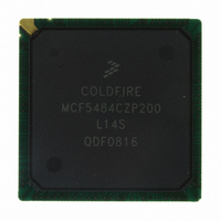
MCF5484CZP200 Freescale Semiconductor, MCF5484CZP200 Datasheet - Page 26

MCF5484CZP200
Manufacturer Part Number
MCF5484CZP200
Description
IC MPU 32BIT COLDF 388-PBGA
Manufacturer
Freescale Semiconductor
Series
MCF548xr
Datasheet
1.MCF5480CVR166.pdf
(34 pages)
Specifications of MCF5484CZP200
Core Processor
Coldfire V4E
Core Size
32-Bit
Speed
200MHz
Connectivity
CAN, EBI/EMI, Ethernet, I²C, SPI, UART/USART, USB
Peripherals
DMA, PWM, WDT
Number Of I /o
99
Program Memory Type
ROMless
Ram Size
32K x 8
Voltage - Supply (vcc/vdd)
1.43 V ~ 1.58 V
Oscillator Type
External
Operating Temperature
-40°C ~ 85°C
Package / Case
388-BGA
Program Memory Size
64KB
Cpu Speed
200MHz
Embedded Interface Type
I2C, UART, DMA
Digital Ic Case Style
BGA
No. Of Pins
388
Supply Voltage Range
3V To 3.6V, 1.43V To 1.58V
Rohs Compliant
No
For Use With
M5485EVBGHSE - KIT DEV GHS FOR M5485EVBM5485EVBGHS - KIT DEV GHS FOR M5485EVBM5485BFEE - MODULE MCF5485 FIRE ENGINEM5485AFEE - MODULE MCF5485 FIRE ENGINEM5485AFE - MODULE MCF5485 FIRE ENGINEM5484GFEE - MODULE M5484 FIRE ENGINEM5484LITEKITE - KIT DEV FOR MCF548X FAMILY
Lead Free Status / RoHS Status
Contains lead / RoHS non-compliant
Eeprom Size
-
Program Memory Size
-
Data Converters
-
Available stocks
Company
Part Number
Manufacturer
Quantity
Price
Company:
Part Number:
MCF5484CZP200
Manufacturer:
Exar
Quantity:
100
Company:
Part Number:
MCF5484CZP200
Manufacturer:
FREESCAL
Quantity:
185
Company:
Part Number:
MCF5484CZP200
Manufacturer:
Freescale Semiconductor
Quantity:
10 000
JTAG and Boundary Scan Timing
Figure 23
14
26
1
Num
J10
J11
J12
J13
J14
MTMOD is expected to be a static signal. Hence, it is not associated with any timing
J1
J2
J3
J4
J5
J6
J7
J8
J9
shows timing for the values in
JTAG and Boundary Scan Timing
TCLK Frequency of Operation
TCLK Cycle Period
TCLK Clock Pulse Width
TCLK Rise and Fall Times
Boundary Scan Input Data Setup Time to TCLK Rise
Boundary Scan Input Data Hold Time after TCLK Rise
TCLK Low to Boundary Scan Output Data Valid
TCLK Low to Boundary Scan Output High Z
TMS, TDI Input Data Setup Time to TCLK Rise
TMS, TDI Input Data Hold Time after TCLK Rise
TRST Assert Time
TRST Setup Time (Negation) to TCLK High
TCLK Low to TDO Data Valid
TCLK Low to TDO High Z
1
2
3
SDA
SCL
Output numbers depend on the value programmed into the IFDR; an IFDR programmed with the
maximum frequency (IFDR = 0x20) results in minimum output timings as shown in
I
SCL low period. The actual position is affected by the prescale and division values programmed
into the IFDR; however, the numbers given in
Because SCL and SDA are open-collector-type outputs, which the processor can only actively
drive low, the time SCL or SDA take to reach a high level depends on external signal capacitance
and pull-up resistor values.
Specified at a nominal 50-pF load.
2
C interface is designed to scale the actual data transition time to move it to the middle of the
I2
I1
Characteristics
Table 22. JTAG and Boundary Scan Timing
MCF548x ColdFire
I4
Table 20
Figure 23. I
and
1
Table
I7
2
C Input/Output Timings
®
21.
Microprocessor, Rev. 4
Table 21
I6
I8
are minimum values.
I5
Symbol
t
t
t
t
t
t
t
t
TAPBHT
TRSTST
TAPBST
TRSTAT
f
t
BSDST
BSDHT
t
t
TDODV
TDODZ
t
t
BSDV
BSDZ
JCYC
JCYC
JCRF
JCW
15.15
100.0
I3
24.0
10.0
10.0
Min
DC
0.0
5.0
0.0
0.0
5.0
0.0
0.0
2
Table
Freescale Semiconductor
Max
15.0
15.0
20.0
15.0
3.0
21. The
10
—
—
—
—
—
—
—
—
I9
MHz
Unit
t
ns
ns
ns
ns
ns
ns
ns
ns
ns
ns
ns
ns
CK


