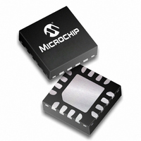
PIC16F688-E/ML Microchip Technology, PIC16F688-E/ML Datasheet - Page 131

PIC16F688-E/ML
Manufacturer Part Number
PIC16F688-E/ML
Description
IC PIC MCU FLASH 4KX14 16QFN
Manufacturer
Microchip Technology
Series
PIC® 16Fr
Datasheets
1.PIC16F616T-ISL.pdf
(8 pages)
2.PIC16F688T-ISL.pdf
(204 pages)
3.PIC16F688T-ISL.pdf
(6 pages)
4.PIC16F688T-ISL.pdf
(4 pages)
5.PIC16F688T-ISL.pdf
(688 pages)
Specifications of PIC16F688-E/ML
Core Size
8-Bit
Program Memory Size
7KB (4K x 14)
Core Processor
PIC
Speed
20MHz
Connectivity
UART/USART
Peripherals
Brown-out Detect/Reset, POR, WDT
Number Of I /o
12
Program Memory Type
FLASH
Eeprom Size
256 x 8
Ram Size
256 x 8
Voltage - Supply (vcc/vdd)
2 V ~ 5.5 V
Data Converters
A/D 8x10b
Oscillator Type
Internal
Operating Temperature
-40°C ~ 125°C
Package / Case
16-QFN
Controller Family/series
PIC16F
No. Of I/o's
12
Eeprom Memory Size
256Byte
Ram Memory Size
256Byte
Cpu Speed
20MHz
No. Of Timers
2
Processor Series
PIC16F
Core
PIC
Data Bus Width
8 bit
Data Ram Size
256 B
Interface Type
EUSART, RS- 232, SCI, USB
Maximum Clock Frequency
20 MHz
Number Of Programmable I/os
12
Number Of Timers
2
Maximum Operating Temperature
+ 125 C
Mounting Style
SMD/SMT
3rd Party Development Tools
52715-96, 52716-328, 52717-734
Development Tools By Supplier
PG164130, DV164035, DV244005, DV164005, PG164120, ICE2000, DM163014, DM164120-4
Minimum Operating Temperature
- 40 C
On-chip Adc
10 bit, 8 Channel
Lead Free Status / RoHS Status
Lead free / RoHS Compliant
For Use With
AC164324 - MODULE SKT FOR MPLAB 8DFN/16QFNXLT16QFN1 - SOCKET TRANSITION 14DIP TO 16QFNAC162061 - HEADER INTRFC MPLAB ICD2 20PINAC162056 - HEADER INTERFACE ICD2 16F688
Lead Free Status / Rohs Status
Details
12.0
The PIC16F688 instruction set is highly orthogonal and
is comprised of three basic categories:
• Byte-oriented operations
• Bit-oriented operations
• Literal and control operations
Each PIC16 instruction is a 14-bit word divided into an
opcode, which specifies the instruction type and one or
more operands, which further specify the operation of
the instruction. The formats for each of the categories
is presented in Figure 12-1, while the various opcode
fields are summarized in Table 12-1.
Table 12-2 lists the instructions recognized by the
MPASM
For byte-oriented instructions, ‘f’ represents a file
register designator and ‘d’ represents a destination
designator. The file register designator specifies which
file register is to be used by the instruction.
The destination designator specifies where the result of
the operation is to be placed. If ‘d’ is zero, the result is
placed in the W register. If ‘d’ is one, the result is placed
in the file register specified in the instruction.
For bit-oriented instructions, ‘b’ represents a bit field
designator, which selects the bit affected by the
operation, while ‘f’ represents the address of the file in
which the bit is located.
For literal and control operations, ‘k’ represents an
8-bit or 11-bit constant, or literal value.
One instruction cycle consists of four oscillator periods;
for an oscillator frequency of 4 MHz, this gives a
nominal instruction execution time of 1 μs. All
instructions are executed within a single instruction
cycle, unless a conditional test is true, or the program
counter is changed as a result of an instruction. When
this occurs, the execution takes two instruction cycles,
with the second cycle executed as a NOP.
All instruction examples use the format ‘0xhh’ to
represent a hexadecimal number, where ‘h’ signifies a
hexadecimal digit.
12.1
Any instruction that specifies a file register as part of
the instruction performs a Read-Modify-Write (R-M-W)
operation. The register is read, the data is modified,
and the result is stored according to either the instruc-
tion, or the destination designator ‘d’. A read operation
is performed on a register even if the instruction writes
to that register.
For example, a CLRF
PORTA, clear all the data bits, then write the result
back to PORTA. This example would have the
unintended consequence of clearing the condition that
set the RAIF flag.
© 2009 Microchip Technology Inc.
TM
INSTRUCTION SET SUMMARY
Read-Modify-Write Operations
assembler.
PORTA instruction will read
TABLE 12-1:
FIGURE 12-1:
Field
DC
PC
TO
PD
W
C
b
d
Z
k
x
f
Byte-oriented file register operations
Bit-oriented file register operations
Literal and control operations
General
CALL and GOTO instructions only
13
13
13
13
Register file address (0x00 to 0x7F)
Working register (accumulator)
Bit address within an 8-bit file register
Literal field, constant data or label
Don’t care location (= 0 or 1).
The assembler will generate code with x = 0.
It is the recommended form of use for
compatibility with all Microchip software tools.
Destination select; d = 0: store result in
d = 1: store result in file register f.
Default is d = 1.
Program Counter
Time-out bit
Carry bit
Digit carry bit
Zero bit
Power-down bit
OPCODE
d = 0 for destination W
d = 1 for destination f
f = 7-bit file register address
b = 3-bit bit address
f = 7-bit file register address
k = 8-bit immediate value
k = 11-bit immediate value
OPCODE
OPCODE
OPCODE
11
OPCODE FIELD
DESCRIPTIONS
10
10 9
GENERAL FORMAT FOR
INSTRUCTIONS
8
Description
b (BIT #)
PIC16F688
7
d
8
6
7
7 6
k (literal)
DS41203E-page 129
f (FILE #)
k (literal)
f (FILE #)
W
0
0
0
0
,


