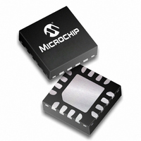
PIC16F688-E/ML Microchip Technology, PIC16F688-E/ML Datasheet - Page 90

PIC16F688-E/ML
Manufacturer Part Number
PIC16F688-E/ML
Description
IC PIC MCU FLASH 4KX14 16QFN
Manufacturer
Microchip Technology
Series
PIC® 16Fr
Datasheets
1.PIC16F616T-ISL.pdf
(8 pages)
2.PIC16F688T-ISL.pdf
(204 pages)
3.PIC16F688T-ISL.pdf
(6 pages)
4.PIC16F688T-ISL.pdf
(4 pages)
5.PIC16F688T-ISL.pdf
(688 pages)
Specifications of PIC16F688-E/ML
Core Size
8-Bit
Program Memory Size
7KB (4K x 14)
Core Processor
PIC
Speed
20MHz
Connectivity
UART/USART
Peripherals
Brown-out Detect/Reset, POR, WDT
Number Of I /o
12
Program Memory Type
FLASH
Eeprom Size
256 x 8
Ram Size
256 x 8
Voltage - Supply (vcc/vdd)
2 V ~ 5.5 V
Data Converters
A/D 8x10b
Oscillator Type
Internal
Operating Temperature
-40°C ~ 125°C
Package / Case
16-QFN
Controller Family/series
PIC16F
No. Of I/o's
12
Eeprom Memory Size
256Byte
Ram Memory Size
256Byte
Cpu Speed
20MHz
No. Of Timers
2
Processor Series
PIC16F
Core
PIC
Data Bus Width
8 bit
Data Ram Size
256 B
Interface Type
EUSART, RS- 232, SCI, USB
Maximum Clock Frequency
20 MHz
Number Of Programmable I/os
12
Number Of Timers
2
Maximum Operating Temperature
+ 125 C
Mounting Style
SMD/SMT
3rd Party Development Tools
52715-96, 52716-328, 52717-734
Development Tools By Supplier
PG164130, DV164035, DV244005, DV164005, PG164120, ICE2000, DM163014, DM164120-4
Minimum Operating Temperature
- 40 C
On-chip Adc
10 bit, 8 Channel
Lead Free Status / RoHS Status
Lead free / RoHS Compliant
For Use With
AC164324 - MODULE SKT FOR MPLAB 8DFN/16QFNXLT16QFN1 - SOCKET TRANSITION 14DIP TO 16QFNAC162061 - HEADER INTRFC MPLAB ICD2 20PINAC162056 - HEADER INTERFACE ICD2 16F688
Lead Free Status / Rohs Status
Details
PIC16F688
10.1.2
The Asynchronous mode would typically be used in
RS-232 systems. The receiver block diagram is shown
in Figure 10-2. The data is received on the RX/DT pin
and drives the data recovery block. The data recovery
block is actually a high-speed shifter operating at 16
times the baud rate, whereas the serial Receive Shift
Register (RSR) operates at the bit rate. When all 8 or 9
bits of the character have been shifted in, they are
immediately transferred to a two character First-In-
First-Out (FIFO) memory. The FIFO buffering allows
reception of two complete characters and the start of a
third character before software must start servicing the
EUSART receiver. The FIFO and RSR registers are not
directly accessible by software. Access to the received
data is via the RCREG register.
10.1.2.1
The EUSART receiver is enabled for asynchronous
operation by configuring the following three control bits:
• CREN = 1
• SYNC = 0
• SPEN = 1
All other EUSART control bits are assumed to be in
their default state.
Setting the CREN bit of the RCSTA register enables the
receiver circuitry of the EUSART. Clearing the SYNC bit
of the TXSTA register configures the EUSART for
asynchronous operation. Setting the SPEN bit of the
RCSTA
automatically configures the RX/DT I/O pin as an input.
If the RX/DT pin is shared with an analog peripheral the
analog I/O function must be disabled by clearing the
corresponding ANSEL bit.
DS41203E-page 88
Note:
register
EUSART ASYNCHRONOUS
RECEIVER
When the SPEN bit is set the TX/CK I/O
pin is automatically configured as an
output, regardless of the state of the
corresponding TRIS bit and whether or not
the EUSART transmitter is enabled. The
PORT latch is disconnected from the
output driver so it is not possible to use the
TX/CK pin as a general purpose output.
Enabling the Receiver
enables
the
EUSART
and
10.1.2.2
The receiver data recovery circuit initiates character
reception on the falling edge of the first bit. The first bit,
also known as the Start bit, is always a zero. The data
recovery circuit counts one-half bit time to the center of
the Start bit and verifies that the bit is still a zero. If it is
not a zero then the data recovery circuit aborts
character reception, without generating an error, and
resumes looking for the falling edge of the Start bit. If
the Start bit zero verification succeeds then the data
recovery circuit counts a full bit time to the center of the
next bit. The bit is then sampled by a majority detect
circuit and the resulting ‘0’ or ‘1’ is shifted into the RSR.
This repeats until all data bits have been sampled and
shifted into the RSR. One final bit time is measured and
the level sampled. This is the Stop bit, which is always
a ‘1’. If the data recovery circuit samples a ‘0’ in the
Stop bit position then a framing error is set for this
character, otherwise the framing error is cleared for this
character. See Section 10.1.2.4 “Receive Framing
Error” for more information on framing errors.
Immediately after all data bits and the Stop bit have
been received, the character in the RSR is transferred
to the EUSART receive FIFO and the RCIF interrupt
flag bit of the PIR1 register is set. The top character in
the FIFO is transferred out of the FIFO by reading the
RCREG register.
10.1.2.3
The RCIF interrupt flag bit of the PIR1 register is set
whenever the EUSART receiver is enabled and there is
an unread character in the receive FIFO. The RCIF
interrupt flag bit is read-only, it cannot be set or cleared
by software.
RCIF interrupts are enabled by setting the following
bits:
• RCIE interrupt enable bit of the PIE1 register
• PEIE peripheral interrupt enable bit of the INT-
• GIE global interrupt enable bit of the INTCON
The RCIF interrupt flag bit will be set when there is an
unread character in the FIFO, regardless of the state of
interrupt enable bits.
Note:
CON register
register
If the receive FIFO is overrun, no additional
characters will be received until the overrun
condition is cleared. See Section 10.1.2.5
“Receive Overrun Error” for more
information on overrun errors.
Receiving Data
Receive Interrupts
© 2009 Microchip Technology Inc.


