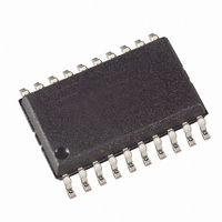
ATTINY26L-8SU Atmel, ATTINY26L-8SU Datasheet - Page 19

ATTINY26L-8SU
Manufacturer Part Number
ATTINY26L-8SU
Description
ID MCU AVR 2K 5V 8MHZ 20-SOIC
Manufacturer
Atmel
Series
AVR® ATtinyr
Specifications of ATTINY26L-8SU
Core Processor
AVR
Core Size
8-Bit
Speed
8MHz
Connectivity
USI
Peripherals
Brown-out Detect/Reset, POR, PWM, WDT
Number Of I /o
16
Program Memory Size
2KB (1K x 16)
Program Memory Type
FLASH
Eeprom Size
128 x 8
Ram Size
128 x 8
Voltage - Supply (vcc/vdd)
2.7 V ~ 5.5 V
Data Converters
A/D 11x10b
Oscillator Type
Internal
Operating Temperature
-40°C ~ 85°C
Package / Case
20-SOIC (7.5mm Width)
Package
20SOIC
Device Core
AVR
Family Name
ATtiny
Maximum Speed
8 MHz
Operating Supply Voltage
3.3|5 V
Data Bus Width
8 Bit
Number Of Programmable I/os
16
Interface Type
SPI/USI
On-chip Adc
11-chx10-bit
Number Of Timers
2
Cpu Family
ATtiny
Device Core Size
8b
Frequency (max)
8MHz
Total Internal Ram Size
128Byte
# I/os (max)
16
Number Of Timers - General Purpose
2
Operating Supply Voltage (typ)
3.3/5V
Operating Supply Voltage (max)
5.5V
Operating Supply Voltage (min)
2.7V
Instruction Set Architecture
RISC
Operating Temp Range
-40C to 85C
Operating Temperature Classification
Industrial
Mounting
Surface Mount
Pin Count
20
Package Type
SOIC
Processor Series
ATTINY2x
Core
AVR8
Data Ram Size
128 B
Maximum Clock Frequency
8 MHz
Maximum Operating Temperature
+ 85 C
Mounting Style
SMD/SMT
3rd Party Development Tools
EWAVR, EWAVR-BL
Development Tools By Supplier
ATAVRDRAGON, ATSTK500, ATSTK600, ATAVRISP2, ATAVRONEKIT
Minimum Operating Temperature
- 40 C
For Use With
ATSTK600-DIP40 - STK600 SOCKET/ADAPTER 40-PDIP770-1007 - ISP 4PORT ATMEL AVR MCU SPI/JTAG770-1004 - ISP 4PORT FOR ATMEL AVR MCU SPIATAVRISP2 - PROGRAMMER AVR IN SYSTEMATSTK505 - ADAPTER KIT FOR 14PIN AVR MCU
Lead Free Status / RoHS Status
Lead free / RoHS Compliant
Other names
ATTINY26L-8SJ
ATTINY26L-8SJ
ATTINY26L-8SJ
Available stocks
Company
Part Number
Manufacturer
Quantity
Price
Company:
Part Number:
ATTINY26L-8SU
Manufacturer:
Atmel
Quantity:
3 500
Part Number:
ATTINY26L-8SU
Manufacturer:
ATMEL/爱特梅尔
Quantity:
20 000
EEPROM Data
Register – EEDR
EEPROM Control
Register – EECR
1477K–AVR–08/10
• Bit 7..0 – EEDR7..0: EEPROM Data
For the EEPROM write operation, the EEDR Register contains the data to be written to the
EEPROM in the address given by the EEAR Register. For the EEPROM read operation, the
EEDR contains the data read out from the EEPROM at the address given by EEAR.
• Bit 7..4 – RES: Reserved Bits
These bits are reserved bits in the ATtiny26(L) and will always read as zero.
• Bit 3 – EERIE: EEPROM Ready Interrupt Enable
When the I-bit in SREG and EERIE are set (one), the EEPROM Ready Interrupt is enabled.
When cleared (zero), the interrupt is disabled. The EEPROM Ready Interrupt generates a con-
stant interrupt when EEWE is cleared (zero).
• Bit 2 – EEMWE: EEPROM Master Write Enable
The EEMWE bit determines whether setting EEWE to one causes the EEPROM to be written.
When EEMWE is set (one), setting EEWE will write data to the EEPROM at the selected
address. If EEMWE is zero, setting EEWE will have no effect. When EEMWE has been set (one)
by software, hardware clears the bit to zero after four clock cycles. See the description of the
EEWE bit for an EEPROM write procedure.
• Bit 1 – EEWE: EEPROM Write Enable
The EEPROM Write Enable Signal – EEWE – is the write strobe to the EEPROM. When
address and data are correctly set up, the EEWE bit must be set to write the value in to the
EEPROM. The EEMWE bit must be set when the logical one is written to EEWE, otherwise no
EEPROM write takes place. The following procedure should be followed when writing the
EEPROM (the order of steps 2 and 3 is unessential):
1. Wait until EEWE becomes zero.
2. Write new EEPROM address to EEAR (optional).
3. Write new EEPROM data to EEDR (optional).
4. Write a logical one to the EEMWE bit in EECR.
5. Within four clock cycles after setting EEMWE, write a logical one to EEWE.
Caution: An interrupt between step 4 and step 5 will make the write cycle fail, since the
EEPROM Master Write Enable will time-out. If an interrupt routine accessing the EEPROM is
interrupting another EEPROM access, the EEAR or EEDR Register will be modified, causing the
interrupted EEPROM access to fail. It is recommended to have the Global Interrupt Flag cleared
during all the steps to avoid these problems.
When the access time (typically 8.3 ms) has elapsed, the EEWE bit is cleared (zero) by hard-
ware. The user software can poll this bit and wait for a zero before writing the next byte. When
EEWE has been set, the CPU is halted for two cycles before the next instruction is executed.
• Bit 0 – EERE: EEPROM Read Enable
Bit
$1D ($3D)
Read/Write
Initial Value
Bit
$1C ($3C)
Read/Write
Initial Value
MSB
R/W
R
7
0
7
–
0
R/W
R
6
0
6
–
0
R/W
R
5
0
5
–
0
R/W
R
4
0
4
–
0
EERIE
R/W
R/W
3
0
3
0
EEMWE
R/W
R/W
2
0
2
0
EEWE
R/W
R/W
1
0
1
0
EERE
LSB
R/W
R/W
0
0
0
0
EEDR
EECR
19


