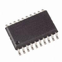
ATTINY461-20SU Atmel, ATTINY461-20SU Datasheet - Page 174

ATTINY461-20SU
Manufacturer Part Number
ATTINY461-20SU
Description
IC MCU AVR 4K FLASH 20MHZ 20SOIC
Manufacturer
Atmel
Series
AVR® ATtinyr
Datasheet
1.ATAVRMC321.pdf
(242 pages)
Specifications of ATTINY461-20SU
Core Processor
AVR
Core Size
8-Bit
Speed
20MHz
Connectivity
USI
Peripherals
Brown-out Detect/Reset, POR, PWM, WDT
Number Of I /o
16
Program Memory Size
4KB (2K x 16)
Program Memory Type
FLASH
Eeprom Size
256 x 8
Ram Size
256 x 8
Voltage - Supply (vcc/vdd)
2.7 V ~ 5.5 V
Data Converters
A/D 11x10b
Oscillator Type
Internal
Operating Temperature
-40°C ~ 85°C
Package / Case
20-SOIC (7.5mm Width)
Processor Series
ATTINY4x
Core
AVR8
Data Bus Width
8 bit
Data Ram Size
256 B
Interface Type
2-Wire, SPI, USI
Maximum Clock Frequency
20 MHz
Number Of Programmable I/os
16
Number Of Timers
2
Operating Supply Voltage
2.7 V to 5.5 V
Maximum Operating Temperature
+ 85 C
Mounting Style
SMD/SMT
3rd Party Development Tools
EWAVR, EWAVR-BL
Development Tools By Supplier
ATAVRDRAGON, ATSTK500, ATSTK600, ATAVRISP2, ATAVRONEKIT
Minimum Operating Temperature
- 40 C
On-chip Adc
10 bit, 16 Channel
Package
20SOIC
Device Core
AVR
Family Name
ATtiny
Maximum Speed
20 MHz
For Use With
ATSTK600-DIP40 - STK600 SOCKET/ADAPTER 40-PDIPATAVRBC100 - REF DESIGN KIT BATTERY CHARGER770-1007 - ISP 4PORT ATMEL AVR MCU SPI/JTAG770-1004 - ISP 4PORT FOR ATMEL AVR MCU SPI
Lead Free Status / RoHS Status
Lead free / RoHS Compliant
Available stocks
Company
Part Number
Manufacturer
Quantity
Price
Company:
Part Number:
ATTINY461-20SU
Manufacturer:
ATMEL
Quantity:
3 282
- Current page: 174 of 242
- Download datasheet (5Mb)
18.6.1
174
ATtiny261/461/861
Serial Programming Algorithm
After RESET is set low, the Programming Enable instruction needs to be executed first before
program/erase operations can be executed.
Table 18-9.
Note:
When programming the EEPROM, an auto-erase cycle is built into the self-timed programming
operation (in the Serial mode ONLY) and there is no need to first execute the Chip Erase
instruction. The Chip Erase operation turns the content of every memory location in both the
Program and EEPROM arrays into 0xFF.
Depending on CKSEL Fuses, a valid clock must be present. The minimum low and high periods
for the serial clock (SCK) input are defined as follows:
When writing serial data to the ATtiny261/461/861, data is clocked on the rising edge of SCK.
When reading, data is clocked on the falling edge of SCK. See
timing details.
To program and verify the ATtiny261/461/861 in the Serial Programming mode, the following
sequence is recommended (see four byte instruction formats in
• Low:> 2 CPU clock cycles for f
• High:> 2 CPU clock cycles for f
1. Power-up sequence:
2. Wait for at least 20 ms and enable serial programming by sending the Programming
3. The serial programming instructions will not work if the communication is out of syn-
4. The Flash is programmed one page at a time. The memory page is loaded one byte at
Apply power between V
tems, the programmer can not guarantee that SCK is held low during power-up. In this
case, RESET must be given a positive pulse after SCK has been set to '0'. The duration
of the pulse must be at least t
19-4 on page
Enable serial instruction to pin MOSI.
chronization. When in sync. the second byte (0x53), will echo back when issuing the
third byte of the Programming Enable instruction. Whether the echo is correct or not, all
four bytes of the instruction must be transmitted. If the 0x53 did not echo back, give
RESET a positive pulse and issue a new Programming Enable command.
a time by supplying the 5 LSB of the address and data together with the Load Program
memory Page instruction. To ensure correct loading of the page, the data low byte must
be loaded before data high byte is applied for a given address. The Program memory
Page is stored by loading the Write Program memory Page instruction with the 6 MSB
of the address. If polling (RDY/BSY) is not used, the user must wait at least t
before issuing the next page. (See
In
dedicated for the internal SPI interface.
Symbol
MOSI
MISO
Table
SCK
Pin Mapping Serial Programming
18-9, above, the pin mapping for SPI programming is listed. Not all parts use the SPI pins
190) plus two CPU clock cycles.
CC
Pins
PB0
PB1
PB2
and GND while RESET and SCK are set to “0”. In some sys-
ck
ck
RST
< 12 MHz, 3 CPU clock cycles for f
< 12 MHz, 3 CPU clock cycles for f
(the minimum pulse width on RESET pin, see
Table
18-10.) Accessing the serial programming
I/O
O
I
I
Table
Figure 19-4
Serial Data out
Serial Data in
18-11):
Description
Serial Clock
ck
ck
>= 12 MHz
>= 12 MHz
and
Figure 19-5
2588E–AVR–08/10
WD_FLASH
Table
for
Related parts for ATTINY461-20SU
Image
Part Number
Description
Manufacturer
Datasheet
Request
R

Part Number:
Description:
Manufacturer:
Atmel Corporation
Datasheet:

Part Number:
Description:
Manufacturer:
Atmel Corporation
Datasheet:

Part Number:
Description:
IC AVR MCU 4K 20MHZ 32-QFN
Manufacturer:
Atmel
Datasheet:

Part Number:
Description:
MCU AVR 4K FLASH 15MHZ 32-QFN
Manufacturer:
Atmel
Datasheet:

Part Number:
Description:
MCU AVR 4KB FLASH 15MHZ 32-VQFN
Manufacturer:
Atmel
Datasheet:

Part Number:
Description:
MCU AVR 4KB FLASH 20MHZ 20SOIC
Manufacturer:
Atmel
Datasheet:

Part Number:
Description:
IC MCU AVR 4K 20MHZ 32QFN
Manufacturer:
Atmel
Datasheet:

Part Number:
Description:
Microcontrollers (MCU) 4kB Flash 0.256kB EEPROM 16 I/O Pins
Manufacturer:
Atmel
Datasheet:

Part Number:
Description:
IC, MCU, 8BIT, 2K FLASH, 20SOIC
Manufacturer:
Atmel
Datasheet:

Part Number:
Description:
IC, MCU, 8BIT, 2K FLASH, 20PDIP
Manufacturer:
Atmel
Datasheet:


