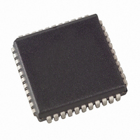
AT89C51RC-24JU Atmel, AT89C51RC-24JU Datasheet - Page 11

AT89C51RC-24JU
Manufacturer Part Number
AT89C51RC-24JU
Description
IC 8051 MCU FLASH 32K 44PLCC
Manufacturer
Atmel
Series
89Cr
Datasheet
1.AT89C51RC-24PU.pdf
(36 pages)
Specifications of AT89C51RC-24JU
Core Processor
8051
Core Size
8-Bit
Speed
24MHz
Connectivity
SPI, UART/USART
Peripherals
WDT
Number Of I /o
32
Program Memory Size
32KB (32K x 8)
Program Memory Type
FLASH
Ram Size
512 x 8
Voltage - Supply (vcc/vdd)
4 V ~ 5.5 V
Oscillator Type
Internal
Operating Temperature
-40°C ~ 85°C
Package / Case
44-PLCC
Package
44PLCC
Device Core
8051
Family Name
89C
Maximum Speed
24 MHz
Operating Supply Voltage
5 V
Data Bus Width
8 Bit
Number Of Programmable I/os
32
Interface Type
UART
Number Of Timers
3
Processor Series
AT89x
Core
8051
Data Ram Size
512 B
Maximum Clock Frequency
33 MHz
Maximum Operating Temperature
+ 85 C
Mounting Style
SMD/SMT
3rd Party Development Tools
PK51, CA51, A51, ULINK2
Minimum Operating Temperature
- 40 C
For Use With
AT89STK-11 - KIT STARTER FOR AT89C51RX2
Lead Free Status / RoHS Status
Lead free / RoHS Compliant
Eeprom Size
-
Data Converters
-
Lead Free Status / Rohs Status
Details
Available stocks
Company
Part Number
Manufacturer
Quantity
Price
Company:
Part Number:
AT89C51RC-24JU
Manufacturer:
ATMEL
Quantity:
34 960
Company:
Part Number:
AT89C51RC-24JU
Manufacturer:
ATMEL
Quantity:
5 000
Part Number:
AT89C51RC-24JU
Manufacturer:
ATMEL/爱特梅尔
Quantity:
20 000
8. Hardware Watchdog Timer (One-time Enabled with Reset-out)
1920D–MICRO–6/08
With EXTRAM = 0, the ERAM is indirectly addressed, using the MOVX instruction in combina-
tion with any of the registers R0, R1 of the selected bank or DPTR. An access to ERAM will not
affect ports P0, P2, P3.6 (WR), and P3.7 (RD). For example, with EXTRAM = 0,
where R0 contains 0A0H, accesses the ERAM at address 0A0H rather than external memory.
An access to external data memory locations higher than FFH (i.e. 0100H to FFFFH) will be per-
formed with the MOVX DPTR instructions in the same way as in the standard 80C51, i.e., with
P0 and P2 as data/address bus, and P3.6 and P3.7 as write and read timing signals (see
7-1).
Figure 7-1.
With EXTRAM = 1, MOVX @ Ri and MOVX@DPTR will be similar to the standard 80C51.
MOVX@Ri will provide an 8-bit address multiplexed with data on Port 0 and any output port pins
can be used to output higher-order address bits. This is to provide the external paging capability.
MOVX@DPTR will generate a 16-bit address. Port 2 outputs the high-order 8 address bits (the
contents of DP0H), while Port 0 multiplexes the low-order 8 address bits (the contents of DP0L)
with data. MOVX@Ri and MOVX@DPTR will generate either read or write signals on P3.6 (WR)
and P3.7 (RD).
The stack pointer (SP) may be located anywhere in the 256 bytes RAM (lower and upper RAM)
internal data memory. The stack may not be located in the ERAM.
The WDT is intended as a recovery method in situations where the CPU may be subjected to
software upsets. The WDT consists of a 13-bit counter and the WatchDog Timer Reset
(WDTRST) SFR. The WDT is defaulted to disable from exiting reset. To enable the WDT, a user
must write 01EH and 0E1H in sequence to the WDTRST register (SFR location 0A6H). When
the WDT is enabled, it will increment every machine cycle while the oscillator is running. The
WDT timeout period is dependent on the external clock frequency. There is no way to disable
the WDT except through reset (either hardware reset or WDT overflow reset). When WDT over-
flows, it will drive an output RESET HIGH pulse at the RST pin.
MOVX@R0, # data
Internal and External Data Memory Address (with EXTRAM = 0)
FF
00
ERAM
256 BYTES
FF
80
00
UPPER
128 BYTES
INTERNAL
RAM
LOWER
128 BYTES
INTERNAL
RAM
FF
80
SPECIAL
FUNCTION
REGISTER
FFFF
0100
0000
EXTERNAL
DATA
MEMORY
AT89C51RC
Figure
11


