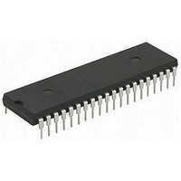
PIC16LF707-I/P Microchip Technology, PIC16LF707-I/P Datasheet - Page 61

PIC16LF707-I/P
Manufacturer Part Number
PIC16LF707-I/P
Description
MCU 8BIT 14KB FLASH 5.5V 40PDIP
Manufacturer
Microchip Technology
Series
PIC® XLP™ 16Fr
Specifications of PIC16LF707-I/P
Core Size
8-Bit
Program Memory Size
14KB (8K x 14)
Peripherals
Brown-out Detect/Reset, POR, PWM, WDT
Core Processor
PIC
Speed
20MHz
Connectivity
I²C, SPI, UART/USART
Number Of I /o
36
Program Memory Type
FLASH
Ram Size
363 x 8
Voltage - Supply (vcc/vdd)
1.8 V ~ 3.6 V
Data Converters
A/D 14x8b
Oscillator Type
Internal
Operating Temperature
-40°C ~ 85°C
Package / Case
40-DIP (0.600", 15.24mm)
Controller Family/series
PIC16LF
No. Of I/o's
36
Ram Memory Size
363Byte
Cpu Speed
20MHz
No. Of Timers
6
Processor Series
PIC16LF
Core
PIC
Data Bus Width
8 bit
Data Ram Size
368 B
Interface Type
I2C, SPI, AUSART
Maximum Clock Frequency
20 MHz
Number Of Programmable I/os
36
Number Of Timers
4
Operating Supply Voltage
1.8 V to 3.6 V
Maximum Operating Temperature
+ 85 C
Mounting Style
Through Hole
3rd Party Development Tools
52715-96, 52716-328, 52717-734
Development Tools By Supplier
PG164130, DV164035, DV244005, DV164005, PG164120, ICE2000
Minimum Operating Temperature
- 40 C
On-chip Adc
8 bit, 14 Channel
On-chip Dac
5 bit
Lead Free Status / RoHS Status
Lead free / RoHS Compliant
Eeprom Size
-
Lead Free Status / Rohs Status
Details
Available stocks
Company
Part Number
Manufacturer
Quantity
Price
Company:
Part Number:
PIC16LF707-I/PT
Manufacturer:
Microchip Technology
Quantity:
10 000
- Current page: 61 of 284
- Download datasheet (3Mb)
6.4.2.3
These pins are configurable to function as one of the
following:
• General purpose I/O
• Capture 1 input, Compare 1 output, and PWM1
• Capacitive sensing input
• TimerB Clock input
6.4.2.4
These pins are configurable to function as one of the
following:
• General purpose I/O
• SPI clock
• I
6.4.2.5
These pins are configurable to function as one of the
following:
• General purpose I/O
• SPI data input
• I
TABLE 6-3:
2010 Microchip Technology Inc.
ANSELC
APFCON
CCP1CON
CCP2CON
CPSACON0
CPSACON1
CPSBCON0
CPSBCON1
PORTC
RCSTA
SSPCON
SSPSTAT
T1CON
TBCON
TXSTA
TRISC
Legend:
output
2
2
C™ clock
C data I/O
Name
x = unknown, u = unchanged, - = unimplemented locations read as ‘0’. Shaded cells are not used by PORTC.
RC2/CCP1/CPSB4/TBCKI
RC3/SCK/SCL
RC4/SDI/SDA
TMR1CS1
CPSAON
CPSBON
TMRBON
TRISC7
ANSC7
WCOL
CSRC
SPEN
Bit 7
SMP
RC7
SUMMARY OF REGISTERS ASSOCIATED WITH PORTC
—
—
—
—
—
TMR1CS0
CPSARM
CPSBRM
TRISC6
SSPOV
ANSC6
Bit 6
CKE
RC6
RX9
TX9
—
—
—
—
—
—
T1CKPS1 T1CKPS0
TRISC5
ANSC5
SSPEN
DC1B1
DC2B1
SREN
TBCS
TXEN
Bit 5
RC5
D/A
—
—
—
—
—
TRISC4
DC1B0
DC2B0
CREN
SYNC
TBSE
Bit 4
RC4
CKP
—
—
—
—
—
—
P
Preliminary
CPSARNG1 CPSARNG0
CPSBRNG1 CPSBRNG0
CPSACH3
CPSBCH3
T1OSCEN
CCP1M3
CCP2M3
ADDEN
TRISC3
SSPM3
TBPSA
PIC16F707/PIC16LF707
Bit 3
RC3
—
—
—
S
6.4.2.6
These pins are configurable to function as one of the
following:
• General purpose I/O
• SPI data output
• Capacitive sensing input
6.4.2.7
These pins are configurable to function as one of the
following:
• General purpose I/O
• Asynchronous serial output
• Synchronous clock I/O
• Capacitive sensing input
6.4.2.8
These pins are configurable to function as one of the
following:
• General purpose I/O
• Asynchronous serial input
• Synchronous serial data I/O
• Capacitive sensing input
CPSACH2
CPSBCH2
CCP1M2
CCP2M2
T1SYNC
TRISC2
SSPM2
ANSC2
TBPS2
BRGH
FERR
Bit 2
RC2
R/W
—
RC5/SDO/CPSA9
RC6/TX/CK/CPSA10
RC7/RX/DT/CPSA11
CPSAOUT
CPSACH1 CPSACH0
CPSBOUT
CPSBCH1 CPSBCH0
CCP1M1
CCP2M1
TRISC1
SSPM1
ANSC1
SSSEL
TBPS1
OERR
TRMT
Bit 1
RC1
UA
—
CCP2SEL
TMR1ON
CCP1M0
CCP2M0
TRISC0
ANSC0
TAXCS
TBXCS
SSPM0
TBPS0
RX9D
TX9D
Bit 0
RC0
BF
0000 00-0
111- -111
---- --00
--00 0000
--00 0000
00-- 0000
---- 0000
00-- 0000
---- 0000
xxxx xxxx
0000 000x
0000 0000
0000 0000
0-00 0000
0000 -010
1111 1111
POR, BOR
Value on
DS41418A-page 61
uuuu uu-u
Value on all
111- -111
---- --00
--00 0000
--00 0000
00-- 0000
---- 0000
00-- 0000
---- 0000
xxxx xxxx
0000 000x
0000 0000
0000 0000
0-00 0000
0000 -010
1111 1111
Resets
other
Related parts for PIC16LF707-I/P
Image
Part Number
Description
Manufacturer
Datasheet
Request
R

Part Number:
Description:
Manufacturer:
Microchip Technology Inc.
Datasheet:

Part Number:
Description:
Manufacturer:
Microchip Technology Inc.
Datasheet:

Part Number:
Description:
Manufacturer:
Microchip Technology Inc.
Datasheet:

Part Number:
Description:
Manufacturer:
Microchip Technology Inc.
Datasheet:

Part Number:
Description:
Manufacturer:
Microchip Technology Inc.
Datasheet:

Part Number:
Description:
Manufacturer:
Microchip Technology Inc.
Datasheet:

Part Number:
Description:
Manufacturer:
Microchip Technology Inc.
Datasheet:

Part Number:
Description:
Manufacturer:
Microchip Technology Inc.
Datasheet:


