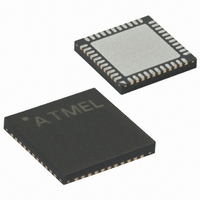
ATMEGA324PA-MU Atmel, ATMEGA324PA-MU Datasheet - Page 21

ATMEGA324PA-MU
Manufacturer Part Number
ATMEGA324PA-MU
Description
MCU AVR 32K FLASH 44-QFN
Manufacturer
Atmel
Series
AVR® ATmegar
Datasheets
1.ATMEGA644PA-PU.pdf
(581 pages)
2.ATMEGA644PA-PU.pdf
(32 pages)
3.ATMEGA164PA-AN.pdf
(30 pages)
Specifications of ATMEGA324PA-MU
Core Processor
AVR
Core Size
8-Bit
Speed
20MHz
Connectivity
I²C, SPI, UART/USART
Peripherals
Brown-out Detect/Reset, POR, PWM, WDT
Number Of I /o
32
Program Memory Size
32KB (16K x 16)
Program Memory Type
FLASH
Eeprom Size
1K x 8
Ram Size
2K x 8
Voltage - Supply (vcc/vdd)
1.8 V ~ 5.5 V
Data Converters
A/D 8x10b
Oscillator Type
Internal
Operating Temperature
-40°C ~ 85°C
Package / Case
44-VQFN Exposed Pad
Processor Series
ATMEGA32x
Core
AVR8
Data Bus Width
8 bit
Data Ram Size
2 KB
Interface Type
2-Wire, SPI, USART
Maximum Clock Frequency
20 MHz
Number Of Programmable I/os
32
Number Of Timers
3
Maximum Operating Temperature
+ 85 C
Mounting Style
SMD/SMT
3rd Party Development Tools
EWAVR, EWAVR-BL
Development Tools By Supplier
ATQT600
Minimum Operating Temperature
- 40 C
On-chip Adc
10 bit, 8 Channel
Controller Family/series
AVR MEGA
No. Of I/o's
32
Eeprom Memory Size
1KB
Ram Memory Size
2KB
Cpu Speed
20MHz
Rohs Compliant
Yes
For Use With
ATSTK600 - DEV KIT FOR AVR/AVR32
Lead Free Status / RoHS Status
Lead free / RoHS Compliant
Available stocks
Company
Part Number
Manufacturer
Quantity
Price
Company:
Part Number:
ATMEGA324PA-MU
Manufacturer:
ATMEL
Quantity:
9 985
- Current page: 21 of 581
- Download datasheet (27Mb)
7.3.1
8272A–AVR–01/10
Data Memory Access Times
The 32 general purpose working registers, 64 I/O registers, 160 Extended I/O Registers and
t h e 1 0 2 4 / 2 0 4 8 / 4 0 9 6 b y t e s o f i n t e r n a l d a t a S R A M i n t h e
ATmega164A/164PA/324A/324PA/644A/644PA/1284/1284P are all accessible through all these
addressing modes. The Register File is described in
13.
Figure 7-2.
This section describes the general access timing concepts for internal memory access. The
internal data SRAM access is performed in two clk
Figure 7-3.
164A/164PA/324A/324PA/644A/644PA/1284/1284P
Address
clk
Data Memory Map for
ATmega164A/164PA/324A/324PA/644A/644PA/1284/1284P
On-chip Data SRAM Access Cycles
Data
Data
WR
CPU
(1024/2048/4096/16384x 8)
RD
160 Ext I/O Reg.
64 I/O Registers
Data Memory
Internal SRAM
32 Registers
Compute Address
T1
Memory Access Instruction
0x0000 - 0x001F
0x0100
0x04FF/0x08FF/0x10FF /0x40FF
0x0020 - 0x005F
0x0060 - 0x00FF
Address valid
CPU
T2
”General Purpose Register File” on page
cycles as described in
Next Instruction
T3
Figure
7-3.
21
Related parts for ATMEGA324PA-MU
Image
Part Number
Description
Manufacturer
Datasheet
Request
R

Part Number:
Description:
Manufacturer:
ATMEL Corporation
Datasheet:

Part Number:
Description:
Manufacturer:
Atmel Corporation
Datasheet:

Part Number:
Description:
Manufacturer:
ATMEL Corporation
Datasheet:

Part Number:
Description:
IC AVR MCU 32K 16MHZ 5V 44-QFN
Manufacturer:
Atmel
Datasheet:

Part Number:
Description:
IC AVR MCU 32K 16MHZ 5V 40DIP
Manufacturer:
Atmel
Datasheet:

Part Number:
Description:
IC AVR MCU 32K 16MHZ 5V 44TQFP
Manufacturer:
Atmel
Datasheet:

Part Number:
Description:
IC AVR MCU 32K 16MHZ IND 40-DIP
Manufacturer:
Atmel
Datasheet:

Part Number:
Description:
IC AVR MCU 32K 16MHZ IND 44-TQFP
Manufacturer:
Atmel
Datasheet:

Part Number:
Description:
MCU AVR 32KB FLASH 16MHZ 44TQFP
Manufacturer:
Atmel
Datasheet:

Part Number:
Description:
MCU AVR 32KB FLASH 16MHZ 44QFN
Manufacturer:
Atmel
Datasheet:

Part Number:
Description:
MCU AVR 32K FLASH 16MHZ 44-TQFP
Manufacturer:
Atmel
Datasheet:

Part Number:
Description:
IC AVR MCU 32K 16MHZ COM 40-DIP
Manufacturer:
Atmel
Datasheet:

Part Number:
Description:
IC AVR MCU 32K 16MHZ COM 44-QFN
Manufacturer:
Atmel
Datasheet:


