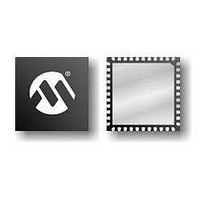
PIC18F47J53T-I/ML Microchip Technology, PIC18F47J53T-I/ML Datasheet - Page 189

PIC18F47J53T-I/ML
Manufacturer Part Number
PIC18F47J53T-I/ML
Description
IC MCU 8BIT 128KB FLASH 44 QFN
Manufacturer
Microchip Technology
Series
PIC® XLP™ 18Fr
Specifications of PIC18F47J53T-I/ML
Program Memory Type
FLASH
Program Memory Size
128KB (64K x 16)
Package / Case
*
Core Processor
PIC
Core Size
8-Bit
Speed
48MHz
Connectivity
I²C, LIN, SPI, UART/USART, USB
Peripherals
Brown-out Detect/Reset, POR, PWM, WDT
Number Of I /o
34
Ram Size
3.8K x 8
Voltage - Supply (vcc/vdd)
2.15 V ~ 3.6 V
Data Converters
A/D 13x10b/12b
Oscillator Type
Internal
Operating Temperature
-40°C ~ 85°C
Processor Series
PIC18F
Core
PIC
Data Bus Width
8 bit
Data Ram Size
3.8 KB
Interface Type
I2C, SPI, USART
Maximum Clock Frequency
48 MHz
Number Of Programmable I/os
22
Number Of Timers
8
Operating Supply Voltage
2.15 V to 3.6 V
Maximum Operating Temperature
+ 85 C
Mounting Style
SMD/SMT
3rd Party Development Tools
52715-96, 52716-328, 52717-734, 52712-325, EWPIC18
Minimum Operating Temperature
- 40 C
Lead Free Status / RoHS Status
Lead free / RoHS Compliant
For Use With
MA180029 - BOARD DEMO PIC18F47J53 FS USB
Eeprom Size
-
Lead Free Status / Rohs Status
Lead free / RoHS Compliant
Available stocks
Company
Part Number
Manufacturer
Quantity
Price
Company:
Part Number:
PIC18F47J53T-I/ML
Manufacturer:
MURATA
Quantity:
640 000
- Current page: 189 of 586
- Download datasheet (6Mb)
11.2.2
When chip select is active and a write strobe occurs
(PMCSx = 1 and PMWR = 1), the data from PMD<7:0>
is captured into the lower PMDIN1L register. The
PMPIF and IBF flag bits are set when the write
ends.The timing for the control signals in Write mode is
displayed in Figure 11-3. The polarity of the control
signals are configurable.
FIGURE 11-3:
FIGURE 11-4:
2010 Microchip Technology Inc.
PMD<7:0>
PMD<7:0>
PMCS1
PMCSx
PMWR
PMWR
PMPIF
PMPIF
PMRD
PMRD
OBE
OBE
IBF
IBF
WRITE TO SLAVE PORT
PARALLEL SLAVE PORT WRITE WAVEFORMS
PARALLEL SLAVE PORT READ WAVEFORMS
Preliminary
PIC18F47J53 FAMILY
11.2.3
When chip select is active and a read strobe occurs
(PMCSx = 1 and PMRD = 1), the data from the
PMDOUT1L register (PMDOUT1L<7:0>) is presented
on to PMD<7:0>. Figure 11-4 provides the timing for
the control signals in Read mode.
|
|
READ FROM SLAVE PORT
Q4
Q4
|
|
Q1
Q1
|
|
Q2
Q2
|
|
DS39964B-page 189
Q3
Q3
|
|
Q4
Q4
Related parts for PIC18F47J53T-I/ML
Image
Part Number
Description
Manufacturer
Datasheet
Request
R

Part Number:
Description:
Manufacturer:
Microchip Technology Inc.
Datasheet:

Part Number:
Description:
Manufacturer:
Microchip Technology Inc.
Datasheet:

Part Number:
Description:
Manufacturer:
Microchip Technology Inc.
Datasheet:

Part Number:
Description:
Manufacturer:
Microchip Technology Inc.
Datasheet:

Part Number:
Description:
Manufacturer:
Microchip Technology Inc.
Datasheet:

Part Number:
Description:
Manufacturer:
Microchip Technology Inc.
Datasheet:

Part Number:
Description:
Manufacturer:
Microchip Technology Inc.
Datasheet:

Part Number:
Description:
Manufacturer:
Microchip Technology Inc.
Datasheet:


