ATMEGA16HVA-4TU Atmel, ATMEGA16HVA-4TU Datasheet - Page 71
ATMEGA16HVA-4TU
Manufacturer Part Number
ATMEGA16HVA-4TU
Description
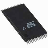
MCU AVR 16K FLASH 4MHZ 28-TSOP
Manufacturer
Atmel
Series
AVR® ATmegar
Datasheet
1.ATMEGA16HVA-4CKU.pdf
(196 pages)
Specifications of ATMEGA16HVA-4TU
Core Processor
AVR
Core Size
8-Bit
Speed
4MHz
Connectivity
SPI
Peripherals
Brown-out Detect/Reset, POR, PWM, WDT
Number Of I /o
7
Program Memory Size
16KB (8K x 16)
Program Memory Type
FLASH
Eeprom Size
256 x 8
Ram Size
512 x 8
Voltage - Supply (vcc/vdd)
1.8 V ~ 9 V
Data Converters
A/D 5x12b
Oscillator Type
External
Operating Temperature
-20°C ~ 85°C
Package / Case
28-TSOP
For Use With
ATSTK600 - DEV KIT FOR AVR/AVR32ATSTK500 - PROGRAMMER AVR STARTER KIT
Lead Free Status / RoHS Status
Lead free / RoHS Compliant
Available stocks
Company
Part Number
Manufacturer
Quantity
Price
Company:

Part Number:
ATMEGA16HVA-4TU
Manufacturer:
Atmel
Quantity:
20


15.3.2
8024A–AVR–04/08
Alternate Functions of Port B
The Port B pins with alternate functions are shown in
Table 15-5.
The alternate pin configuration is as follows:
• MISO/INT2 - Port B, Bit 3
MISO, Master Data input: Slave Data output pin for SPI channel. When the SPI is enabled as a
Master, this pin is configured as an input regardless of the setting of DDB3. When the SPI is
enabled as a Slave, the data direction of this pin is controlled by DDB3. When the pin is forced
by the SPI to be an input, the pull-up can still be controlled by the PORTB3 bit. When not operat-
ing in SPI mode, this pin can serve as an external interrupt source.
• MOSI/INT1- Port B, Bit 2
MOSI, SPI Master Data output: Slave Data input for SPI channel. When the SPI is enabled as a
Slave, this pin is configured as an input regardless of the setting of DDB2. When the SPI is
enabled as a Master, the data direction of this pin is controlled by DDB2. When the pin is forced
by the SPI to be an input, the pull-up can still be controlled by the PORTB2 bit. When not operat-
ing in SPI mode, this pin can serve as an external interrupt source.
• SCK- Port B, Bit 1
SCK, Master Clock output: Slave Clock input pin for SPI channel. When the SPI is enabled as a
Slave, this pin is configured as an input regardless of the setting of DDB1. When the SPI is
enabled as a Master, the data direction of this pin is controlled by DDB1. When the pin is forced
by the SPI to be an input, the pull-up can still be controlled by the PORTB1 bit.
• SS/CKOUT- Port B, Bit 0
SS, Slave Select input: When the SPI is enabled as a Slave, this pin is configured as an input
regardless of the setting of DDB0. As a Slave, the SPI is activated when this pin is driven low.
When the SPI is enabled as a Master, the data direction of this pin is controlled by DDB0. When
the pin is forced by the SPI to be an input, the pull-up can still be controlled by the PORTB0 bit.
When not operating in SPI mode, this pin can serve as Clock Output, CPU Clock divided by 2.
See
Port Pin
PB3
PB2
PB1
PB0
”Clock Output” on page
Alternate Functions
MISO/ INT2 (SPI Bus Master Input/Slave Output or External Interrupt 2 Input)
MOSI/ INT1 (SPI Bus Master Output/Slave Input or External Interrupt 1 Input)
SCK (SPI Bus Master clock Input)
SS/ CKOUT (SPI Bus Master Slave select or Clock Output)
Port B Pins Alternate Functions
27.
Table
ATmega8HVA/16HVA
15-5.
71
Related parts for ATMEGA16HVA-4TU
Image
Part Number
Description
Manufacturer
Datasheet
Request
R

Part Number:
Description:
Manufacturer:
Atmel Corporation
Datasheet:

Part Number:
Description:
IC AVR MCU 16K 16MHZ 5V 44TQFP
Manufacturer:
Atmel
Datasheet:

Part Number:
Description:
IC AVR MCU 16K 16MHZ 5V 44-QFN
Manufacturer:
Atmel
Datasheet:

Part Number:
Description:
IC AVR MCU 16K 16MHZ 5V 40DIP
Manufacturer:
Atmel
Datasheet:
Part Number:
Description:
MCU AVR 16K FLASH 16MHZ 44-QFN
Manufacturer:
Atmel
Datasheet:
Part Number:
Description:
IC AVR MCU 16K 16MHZ COM 40-DIP
Manufacturer:
Atmel
Datasheet:
Part Number:
Description:
IC AVR MCU 16K 16MHZ COM 44-QFN
Manufacturer:
Atmel
Datasheet:
Part Number:
Description:
IC AVR MCU 16K 16MHZ IND 40-DIP
Manufacturer:
Atmel
Datasheet:
Part Number:
Description:
IC AVR MCU 16K 16MHZ IND 44-QFN
Manufacturer:
Atmel
Datasheet:
Part Number:
Description:
IC AVR MCU 16K 16MHZ IND 44-TQFP
Manufacturer:
Atmel
Datasheet:
Part Number:
Description:
IC MCU 8BIT 16KB FLASH 44TQFP
Manufacturer:
Atmel
Datasheet:
Part Number:
Description:
MCU AVR 16K FLASH 16MHZ 44-TQFP
Manufacturer:
Atmel
Datasheet:
Part Number:
Description:
IC AVR MCU 16K 16MHZ COM 44-TQFP
Manufacturer:
Atmel
Datasheet: