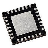
PIC18F27J13-I/ML Microchip Technology, PIC18F27J13-I/ML Datasheet - Page 415

PIC18F27J13-I/ML
Manufacturer Part Number
PIC18F27J13-I/ML
Description
IC PIC MCU 128KB FLASH 28QFN
Manufacturer
Microchip Technology
Series
PIC® XLP™ 18Fr
Datasheets
1.PIC18LF24J10-ISS.pdf
(32 pages)
2.PIC18F26J13-ISS.pdf
(496 pages)
3.PIC18F26J13-ISS.pdf
(558 pages)
4.PIC18F26J13-ISS.pdf
(12 pages)
Specifications of PIC18F27J13-I/ML
Core Size
8-Bit
Program Memory Size
128KB (64K x 16)
Core Processor
PIC
Speed
48MHz
Connectivity
I²C, LIN, SPI, UART/USART
Peripherals
Brown-out Detect/Reset, POR, PWM, WDT
Number Of I /o
22
Program Memory Type
FLASH
Ram Size
3.8K x 8
Voltage - Supply (vcc/vdd)
2.15 V ~ 3.6 V
Data Converters
A/D 10x10b/12b
Oscillator Type
Internal
Operating Temperature
-40°C ~ 85°C
Package / Case
*
Controller Family/series
PIC18
Cpu Speed
48MHz
Digital Ic Case Style
QFN
Supply Voltage Range
1.8V To 5.5V
Embedded Interface Type
I2C, SPI, USART
Rohs Compliant
Yes
Processor Series
PIC18F
Core
PIC
Data Bus Width
8 bit
Data Ram Size
4 KB
Interface Type
I2C, SPI, EUSART
Maximum Clock Frequency
48 MHz
Number Of Programmable I/os
19
Number Of Timers
8
Operating Supply Voltage
2 V to 3.6 V
Maximum Operating Temperature
+ 85 C
Mounting Style
SMD/SMT
3rd Party Development Tools
52715-96, 52716-328, 52717-734, 52712-325, EWPIC18
Development Tools By Supplier
DM164128, DM180021, DM183026-2, DV164131, MA180030, DM183022, DM183032, DV164136, MA180024
Minimum Operating Temperature
- 40 C
On-chip Adc
12 bit, 10 Channel
Lead Free Status / RoHS Status
Lead free / RoHS Compliant
For Use With
MA180030 - BOARD DEMO PIC18F47J13 FS USBMA180029 - BOARD DEMO PIC18F47J53 FS USB
Eeprom Size
-
Lead Free Status / Rohs Status
Details
Available stocks
Company
Part Number
Manufacturer
Quantity
Price
Company:
Part Number:
PIC18F27J13-I/ML
Manufacturer:
MICROCHIP
Quantity:
4 000
- PIC18LF24J10-ISS PDF datasheet
- PIC18F26J13-ISS PDF datasheet #2
- PIC18F26J13-ISS PDF datasheet #3
- PIC18F26J13-ISS PDF datasheet #4
- Current page: 415 of 558
- Download datasheet (5Mb)
27.0
PIC18F47J13 family devices include several features
intended to maximize reliability and minimize cost
through elimination of external components. These are:
• Oscillator Selection
• Resets:
• Interrupts
• Watchdog Timer (WDT)
• Fail-Safe Clock Monitor (FSCM)
• Two-Speed Start-up
• Code Protection
• In-Circuit Serial Programming (ICSP)
The oscillator can be configured for the application
depending on frequency, power, accuracy and cost. All
of the options are discussed in detail in Section 3.0
“Oscillator Configurations”.
A complete discussion of device Resets and interrupts
is available in previous sections of this data sheet. In
addition to their Power-up and Oscillator Start-up
Timers provided for Resets, the PIC18F47J13 family of
devices has a configurable Watchdog Timer (WDT),
which is controlled in software.
The inclusion of an internal RC oscillator also provides
the additional benefits of a Fail-Safe Clock Monitor
(FSCM) and Two-Speed Start-up. FSCM provides for
background monitoring of the peripheral clock and
automatic switchover in the event of its failure.
Two-Speed Start-up enables code to be executed
almost immediately on start-up, while the primary clock
source completes its start-up delays.
All of these features are enabled and configured by
setting the appropriate Configuration register bits.
27.1
The Configuration bits can be programmed to select
various device configurations. The configuration data is
stored in the last four words of Flash program memory;
Figure 6-1 depicts this. The configuration data gets
loaded into the volatile Configuration registers,
CONFIG1L through CONFIG4H, which are readable
and mapped to program memory, starting at location
300000h.
Table 27-2 provides a complete list of the Configuration
bits and Device IDs. A detailed explanation of the vari-
ous bit functions is provided in Register 27-1 through
Register 27-6.
2010 Microchip Technology Inc.
- Power-on Reset (POR)
- Power-up Timer (PWRT)
- Oscillator Start-up Timer (OST)
- Brown-out Reset (BOR)
SPECIAL FEATURES OF THE
CPU
Configuration Bits
Preliminary
PIC18F47J13 FAMILY
27.1.1
Unlike
PIC18F47J13 family devices do not use persistent
memory registers to store configuration information.
The Configuration registers, CONFIG1L through
CONFIG4H, are implemented as volatile memory.
Immediately after power-up, or after a device Reset,
the microcontroller hardware automatically loads the
CONFIG1L through CONFIG4L registers with configu-
ration data stored in nonvolatile Flash program
memory. The last four words of Flash program memory,
known as the Flash Configuration Words (FCW), are
used to store the configuration data.
Table 27-1 provides the Flash program memory, which
will be loaded into the corresponding Configuration
register.
When creating applications for these devices, users
should always specifically allocate the location of the
FCW for configuration data. This is to make certain that
program code is not stored in this address when the
code is compiled.
The four Most Significant bits (MSb) of the FCW, corre-
sponding to CONFIG1H, CONFIG2H, CONFIG3H and
CONFIG4H, should always be programmed to ‘1111’.
This makes these FCWs appear to be NOP instructions
in the remote event that their locations are ever
executed by accident.
The four MSbs of the CONFIG1H, CONFIG2H,
CONFIG3H
implemented, so writing ‘1’s to their corresponding
FCW has no effect on device operation.
To prevent inadvertent configuration changes during
code
CONFIG1L through CONFIG4L, are loaded only once
per power-up or Reset cycle. User’s firmware can still
change the configuration by using self-reprogramming
to modify the contents of the FCW.
Modifying the FCW will not change the active contents
being used in the CONFIG1L through CONFIG4H
registers until after the device is reset.
execution,
some
CONSIDERATIONS FOR
CONFIGURING THE PIC18F47J13
FAMILY DEVICES
and
previous
CONFIG4H
the
Configuration
PIC18
registers
DS39974A-page 415
microcontrollers,
registers,
are
not
Related parts for PIC18F27J13-I/ML
Image
Part Number
Description
Manufacturer
Datasheet
Request
R

Part Number:
Description:
Manufacturer:
Microchip Technology Inc.
Datasheet:

Part Number:
Description:
Manufacturer:
Microchip Technology Inc.
Datasheet:

Part Number:
Description:
Manufacturer:
Microchip Technology Inc.
Datasheet:

Part Number:
Description:
Manufacturer:
Microchip Technology Inc.
Datasheet:

Part Number:
Description:
Manufacturer:
Microchip Technology Inc.
Datasheet:

Part Number:
Description:
Manufacturer:
Microchip Technology Inc.
Datasheet:

Part Number:
Description:
Manufacturer:
Microchip Technology Inc.
Datasheet:

Part Number:
Description:
Manufacturer:
Microchip Technology Inc.
Datasheet:


