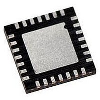
PIC18LF27J53-I/ML Microchip Technology, PIC18LF27J53-I/ML Datasheet - Page 335

PIC18LF27J53-I/ML
Manufacturer Part Number
PIC18LF27J53-I/ML
Description
IC PIC MCU 128KB FLASH 28QFN
Manufacturer
Microchip Technology
Series
PIC® XLP™ 18Fr
Datasheets
1.PIC18LF24J10-ISS.pdf
(32 pages)
2.PIC18F26J13-ISS.pdf
(496 pages)
3.PIC18F26J53-ISS.pdf
(586 pages)
4.PIC18F26J53-ISS.pdf
(12 pages)
Specifications of PIC18LF27J53-I/ML
Core Size
8-Bit
Program Memory Size
128KB (64K x 16)
Core Processor
PIC
Speed
48MHz
Connectivity
I²C, LIN, SPI, UART/USART, USB
Peripherals
Brown-out Detect/Reset, POR, PWM, WDT
Number Of I /o
22
Program Memory Type
FLASH
Ram Size
3.8K x 8
Voltage - Supply (vcc/vdd)
2 V ~ 2.75 V
Data Converters
A/D 10x10b/12b
Oscillator Type
Internal
Operating Temperature
-40°C ~ 85°C
Package / Case
*
Controller Family/series
PIC18
Cpu Speed
48MHz
Digital Ic Case Style
QFN
Supply Voltage Range
1.8V To 3.6V
Embedded Interface Type
I2C, SPI, USART
Rohs Compliant
Yes
Lead Free Status / RoHS Status
Lead free / RoHS Compliant
Eeprom Size
-
Lead Free Status / RoHS Status
Lead free / RoHS Compliant, Lead free / RoHS Compliant
Available stocks
Company
Part Number
Manufacturer
Quantity
Price
Company:
Part Number:
PIC18LF27J53-I/ML
Manufacturer:
ATMEL
Quantity:
101
- PIC18LF24J10-ISS PDF datasheet
- PIC18F26J13-ISS PDF datasheet #2
- PIC18F26J53-ISS PDF datasheet #3
- PIC18F26J53-ISS PDF datasheet #4
- Current page: 335 of 496
- Download datasheet (5Mb)
TABLE 20-1:
REGISTER 20-1:
2010 Microchip Technology Inc.
bit 7
Legend:
R = Readable bit
-n = Value at POR
bit 7
bit 6-4
bit 3
bit 2
bit 1
bit 0
Note 1:
SRCLK<2:0>
SRLEN
R/W-0
111
110
101
100
011
010
001
000
2:
Changing the SRCLK bits while the SR latch is enabled may cause false triggers to the set and Reset
inputs of the latch.
Set only, always reads back ‘0’.
SRLEN: SR Latch Enable bit
1 = SR latch is enabled
0 = SR latch is disabled
SRCLK<2:0>: SR Latch Clock Divider Bits
000 = Generates a 2 T
001 = Generates a 2 T
010 = Generates a 2 T
011 = Generates a 2 T
100 = Generates a 2 T
101 = Generates a 2 T
110 = Generates a 2 T
111 = Generates a 2 T
SRQEN: SR Latch Q Output Enable bit
1 = Q is present on the SRQ pin
0 = Q is internal only
SRNQEN: SR Latch Q Output Enable bit
1 = Q is present on the SRNQ pin
0 = Q is internal only
SRPS: Pulse Set Input of the SR Latch bit
1 = Pulse set input for 2 T
0 = No effect on set input
SRPR: Pulse Reset Input of the SR Latch bit
1 = Pulse reset input for 2 T
0 = No effect on Reset input
DIVSRCLK FREQUENCY TABLE
Divider
R/W-0
512
256
128
64
32
16
8
4
SRCON0: SR LATCH CONTROL REGISTER
SRCLK<2:0>
F
W = Writable bit
‘1’ = Bit is set
OSC
R/W-0
25.6 s
12.8 s
6.4 s
3.2 s
1.6 s
0.8 s
0.4 s
0.2 s
= 20 MHz
OSC
OSC
OSC
OSC
OSC
OSC
OSC
OSC
OSC
OSC
wide pulse on DIVSRCLK every 4 peripheral clock cycles
wide pulse on DIVSRCLK every 16 peripheral clock cycles
wide pulse on DIVSRCLK every 32 peripheral clock cycles
wide pulse on DIVSRCLK every 64 peripheral clock cycles
wide pulse on DIVSRCLK every 128 peripheral clock cycles
wide pulse on DIVSRCLK every 256 peripheral clock cycles
wide pulse on DIVSRCLK every 512 peripheral clock cycles
(1)
wide pulse on DIVSRCLK every 8 peripheral clock cycles
clock cycles
R/W-0
clock cycles
F
Preliminary
OSC
0.25 s
0.5 s
32 s
16 s
8 s
4 s
2 s
1 s
= 16 MHz
(2)
U = Unimplemented
‘0’ = Bit is cleared
(2)
SRQEN
R/W-0
PIC18(L)F2X/4XK22
F
OSC
0.5 s
64 s
32 s
16 s
8 s
4 s
2 s
1 s
= 8 MHz F
SRNQEN
R/W-0
OSC
128 s
C = Clearable only bit
x = Bit is unknown
64 s
32 s
16 s
8 s
4 s
2 s
1 s
= 4 MHz
R/W-0
SRPS
DS41412D-page 335
F
OSC
512 s
256 s
128 s
64 s
32 s
16 s
R/W-0
SRPR
8 s
4 s
= 1 MHz
bit 0
Related parts for PIC18LF27J53-I/ML
Image
Part Number
Description
Manufacturer
Datasheet
Request
R

Part Number:
Description:
Manufacturer:
Microchip Technology Inc.
Datasheet:

Part Number:
Description:
Manufacturer:
Microchip Technology Inc.
Datasheet:

Part Number:
Description:
Manufacturer:
Microchip Technology Inc.
Datasheet:

Part Number:
Description:
Manufacturer:
Microchip Technology Inc.
Datasheet:

Part Number:
Description:
Manufacturer:
Microchip Technology Inc.
Datasheet:

Part Number:
Description:
Manufacturer:
Microchip Technology Inc.
Datasheet:

Part Number:
Description:
Manufacturer:
Microchip Technology Inc.
Datasheet:

Part Number:
Description:
Manufacturer:
Microchip Technology Inc.
Datasheet:


