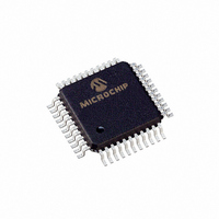
PIC16LC65B-04/PQ Microchip Technology, PIC16LC65B-04/PQ Datasheet - Page 39

PIC16LC65B-04/PQ
Manufacturer Part Number
PIC16LC65B-04/PQ
Description
IC MCU OTP 4KX14 PWM 44-MQFP
Manufacturer
Microchip Technology
Series
PIC® 16Cr
Specifications of PIC16LC65B-04/PQ
Core Processor
PIC
Core Size
8-Bit
Speed
4MHz
Connectivity
I²C, SPI, UART/USART
Peripherals
Brown-out Detect/Reset, POR, PWM, WDT
Number Of I /o
33
Program Memory Size
7KB (4K x 14)
Program Memory Type
OTP
Ram Size
192 x 8
Voltage - Supply (vcc/vdd)
2.5 V ~ 5.5 V
Oscillator Type
External
Operating Temperature
0°C ~ 70°C
Package / Case
44-MQFP, 44-PQFP
Processor Series
PIC16LC
Core
PIC
Data Bus Width
8 bit
Data Ram Size
192 B
Interface Type
I2C, SPI, USART
Maximum Clock Frequency
20 MHz
Number Of Programmable I/os
33
Number Of Timers
3
Operating Supply Voltage
2.5 V to 6 V
Maximum Operating Temperature
+ 70 C
Mounting Style
SMD/SMT
3rd Party Development Tools
52715-96, 52716-328, 52717-734
Development Tools By Supplier
ICE2000, DM163022
Minimum Operating Temperature
0 C
Data Rom Size
192 B
Height
2 mm
Length
10 mm
Supply Voltage (max)
5.5 V
Supply Voltage (min)
3.65 V
Width
10 mm
Lead Free Status / RoHS Status
Lead free / RoHS Compliant
Eeprom Size
-
Data Converters
-
Lead Free Status / Rohs Status
Details
Available stocks
Company
Part Number
Manufacturer
Quantity
Price
Company:
Part Number:
PIC16LC65B-04/PQ
Manufacturer:
SIGMADESI
Quantity:
400
Company:
Part Number:
PIC16LC65B-04/PQ
Manufacturer:
Microchip Technology
Quantity:
10 000
6.0
The Timer0 module timer/counter has the following fea-
tures:
• 8-bit timer/counter
• Readable and writable
• 8-bit software programmable prescaler
• Internal or external clock select
• Interrupt on overflow from FFh to 00h
• Edge select for external clock
Figure 6-1 is a block diagram of the Timer0 module and
the prescaler shared with the WDT.
Additional information on the Timer0 module is
available in the PICmicro™ Mid-Range MCU Family
Reference Manual (DS33023).
Timer mode is selected by clearing bit T0CS
(OPTION_REG<5>). In Timer mode, the Timer0
module will increment every instruction cycle (without
prescaler). If the TMR0 register is written, the incre-
ment is inhibited for the following two instruction cycles.
The user can work around this by writing an adjusted
value to the TMR0 register.
FIGURE 6-1:
RA4/T0CKI
2000 Microchip Technology Inc.
CLKOUT (= F
WDT Enable bit
pin
Watchdog
Note: T0CS, T0SE, PSA, PS2:PS0 are (OPTION_REG<5:0>).
Timer
TIMER0 MODULE
OSC
/4)
T0SE
BLOCK DIAGRAM OF THE TIMER0/WDT PRESCALER
0
1
PSA
M
U
X
0
1
T0CS
M
U
X
0
8-bit Prescaler
8 - to - 1MUX
Time-out
8
M U X
WDT
PIC16C63A/65B/73B/74B
PRESCALER
1
0
1
PSA
M
U
X
Counter mode is selected by setting bit T0CS
(OPTION_REG<5>). In counter mode, Timer0 will
increment, either on every rising, or falling edge of pin
RA4/T0CKI. The incrementing edge is determined by
the
(OPTION_REG<4>). Clearing bit T0SE selects the ris-
ing edge. Restrictions on the external clock input are
discussed in detail in Section 6.2.
The prescaler is mutually exclusively shared between
the Timer0 module and the watchdog timer. The
prescaler is not readable or writable. Section 6.3
details the operation of the prescaler.
6.1
The TMR0 interrupt is generated when the TMR0 reg-
ister overflows from FFh to 00h. This overflow sets bit
T0IF (INTCON<2>). The interrupt can be masked by
clearing bit T0IE (INTCON<5>). Bit T0IF must be
cleared in software by the Timer0 module Interrupt Ser-
vice Routine before re-enabling this interrupt. The
TMR0 interrupt cannot awaken the processor from
SLEEP, since the timer is shut-off during SLEEP.
PSA
Timer0
PS2:PS0
Timer0 Interrupt
Cycles
SYNC
2
Source
Edge
TMR0 reg
Data Bus
8
Select
DS30605C-page 39
Set Flag bit T0IF
on Overflow
bit
T0SE


