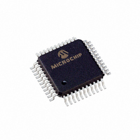
PIC16LC65B-04/PQ Microchip Technology, PIC16LC65B-04/PQ Datasheet - Page 55

PIC16LC65B-04/PQ
Manufacturer Part Number
PIC16LC65B-04/PQ
Description
IC MCU OTP 4KX14 PWM 44-MQFP
Manufacturer
Microchip Technology
Series
PIC® 16Cr
Specifications of PIC16LC65B-04/PQ
Core Processor
PIC
Core Size
8-Bit
Speed
4MHz
Connectivity
I²C, SPI, UART/USART
Peripherals
Brown-out Detect/Reset, POR, PWM, WDT
Number Of I /o
33
Program Memory Size
7KB (4K x 14)
Program Memory Type
OTP
Ram Size
192 x 8
Voltage - Supply (vcc/vdd)
2.5 V ~ 5.5 V
Oscillator Type
External
Operating Temperature
0°C ~ 70°C
Package / Case
44-MQFP, 44-PQFP
Processor Series
PIC16LC
Core
PIC
Data Bus Width
8 bit
Data Ram Size
192 B
Interface Type
I2C, SPI, USART
Maximum Clock Frequency
20 MHz
Number Of Programmable I/os
33
Number Of Timers
3
Operating Supply Voltage
2.5 V to 6 V
Maximum Operating Temperature
+ 70 C
Mounting Style
SMD/SMT
3rd Party Development Tools
52715-96, 52716-328, 52717-734
Development Tools By Supplier
ICE2000, DM163022
Minimum Operating Temperature
0 C
Data Rom Size
192 B
Height
2 mm
Length
10 mm
Supply Voltage (max)
5.5 V
Supply Voltage (min)
3.65 V
Width
10 mm
Lead Free Status / RoHS Status
Lead free / RoHS Compliant
Eeprom Size
-
Data Converters
-
Lead Free Status / Rohs Status
Details
Available stocks
Company
Part Number
Manufacturer
Quantity
Price
Company:
Part Number:
PIC16LC65B-04/PQ
Manufacturer:
SIGMADESI
Quantity:
400
Company:
Part Number:
PIC16LC65B-04/PQ
Manufacturer:
Microchip Technology
Quantity:
10 000
10.0
10.1
The Synchronous Serial Port (SSP) module is a serial
interface useful for communicating with other periph-
eral or microcontroller devices. These peripheral
devices may be Serial EEPROMs, shift registers, dis-
play drivers, A/D converters, etc. The SSP module can
operate in one of two modes:
• Serial Peripheral Interface (SPI)
• Inter-Integrated Circuit (I
An overview of I
tion on the SSP module can be found in the PICmicro™
Mid-Range
(DS33023).
Refer to Application Note AN578, “Use of the SSP
Module in the I
10.2
This section contains register definitions and opera-
tional characteristics of the SPI module.
SPI mode allows 8 bits of data to be synchronously
transmitted and received simultaneously. To accom-
plish communication, typically three pins are used:
• Serial Data Out (SDO) RC5/SDO
• Serial Data In (SDI) RC4/SDI/SDA
• Serial Clock (SCK) RC3/SCK/SCL
Additionally, a fourth pin may be used when in a Slave
mode of operation:
• Slave Select (SS) RA5/SS/AN4
When initializing the SPI, several options need to be
specified. This is done by programming the appropriate
control bits in the SSPCON register (SSPCON<5:0>)
and SSPSTAT<7:6>. These control bits allow the fol-
lowing to be specified:
• Master mode (SCK is the clock output)
• Slave mode (SCK is the clock input)
• Clock Polarity (Idle state of SCK)
• Clock edge (output data on rising/falling edge of
• Clock Rate (Master mode only)
• Slave Select mode (Slave mode only)
SCK)
2000 Microchip Technology Inc.
SYNCHRONOUS SERIAL PORT
(SSP) MODULE
SSP Module Overview
SPI Mode
MCU
2
C Multi-Master Environment.”
2
C operations and additional informa-
Family
2
C)
Reference
Manual
PIC16C63A/65B/73B/74B
FIGURE 10-1:
To enable the serial port, SSP enable bit, SSPEN
(SSPCON<5>) must be set. To reset or reconfigure SPI
mode, clear bit SSPEN, re-initialize the SSPCON reg-
ister, and then set bit SSPEN. This configures the SDI,
SDO, SCK, and SS pins as serial port pins. For the pins
to behave as the serial port function, they must have
their data direction bits (in the TRISC register) appro-
priately programmed. That is:
• SDI must have TRISC<4> set
• SDO must have TRISC<5> cleared
• SCK (Master mode) must have TRISC<3> cleared
• SCK (Slave mode) must have TRISC<3> set
• SS must have TRISA<5> set
• ADCON1 must configure RA5 as a digital I/O pin.
.
RC4/SDI/SDA
RA5/SS/AN4
Note 1: When the SPI is in Slave mode with SS
RC3/SCK/
RC5/SDO
SCL
2: If the SPI is used in Slave mode with
pin control enabled (SSPCON<3:0> =
0100), the SPI module will reset if the SS
pin is set to V
CKE = '1', then the SS pin control must be
enabled.
Read
SS Control
Select
TRISC<3>
Edge
SSP BLOCK DIAGRAM
(SPI MODE)
Enable
SSPM3:SSPM0
bit0
Select
Edge
SSPBUF reg
DD
SSPSR reg
.
Clock Select
4
2
DS30605C-page 55
Prescaler
TMR2 Output
4, 16, 64
Write
Clock
Shift
Data Bus
Internal
2
T
CY


