PIC18LF47J53-I/ML Microchip Technology, PIC18LF47J53-I/ML Datasheet - Page 225
PIC18LF47J53-I/ML
Manufacturer Part Number
PIC18LF47J53-I/ML
Description
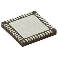
IC PIC MCU 128KB FLASH 44QFN
Manufacturer
Microchip Technology
Series
PIC® XLP™ 18Fr
Datasheets
1.PIC18LF24J10-ISS.pdf
(32 pages)
2.PIC18F26J13-ISS.pdf
(496 pages)
3.PIC18F26J53-ISS.pdf
(586 pages)
4.PIC18F26J53-ISS.pdf
(12 pages)
Specifications of PIC18LF47J53-I/ML
Core Size
8-Bit
Program Memory Size
128KB (64K x 16)
Core Processor
PIC
Speed
48MHz
Connectivity
I²C, LIN, SPI, UART/USART, USB
Peripherals
Brown-out Detect/Reset, POR, PWM, WDT
Number Of I /o
34
Program Memory Type
FLASH
Ram Size
3.8K x 8
Voltage - Supply (vcc/vdd)
2 V ~ 2.75 V
Data Converters
A/D 13x10b/12b
Oscillator Type
Internal
Operating Temperature
-40°C ~ 85°C
Package / Case
*
Controller Family/series
PIC18
Cpu Speed
48MHz
Digital Ic Case Style
QFN
Supply Voltage Range
1.8V To 3.6V
Embedded Interface Type
I2C, SPI, USART
Rohs Compliant
Yes
Lead Free Status / RoHS Status
Lead free / RoHS Compliant
Eeprom Size
-
Lead Free Status / RoHS Status
Lead free / RoHS Compliant, Lead free / RoHS Compliant


15.2
Timer3 and Timer5 can operate in these modes:
• Timer
• Synchronous Counter
• Asynchronous Counter
• Timer with Gated Control
FIGURE 15-1:
2010 Microchip Technology Inc.
Note 1:
SOSCGO
T1OSCEN
T3OSCEN
T5OSCEN
TxG
From Timer4/6
Match PR4/6
Comparator 1
Output
Comparator 2
Output
Timer3/5 Operation
TxGSS<1:0>
2:
3:
T1OSO/T1CKI
ST buffer is a high-speed type when using T1CKI.
Timerx registers increment on rising edge.
Synchronization does not operate while in Sleep.
T
X
OSCEN
TxGPOL
T1OSI
TxCKI
Set flag bit
TMRxIF on
Overflow
TIMER3/5 BLOCK DIAGRAM
00
10
11
01
T1OSC/SOSC
TMRxON
TxGTM
TMRxH
EN
OUT
TMRx
(1)
TxG_IN
(2)
D
R
CK
TMRxL
Q
Q
1
0
Preliminary
TMRxCS<1:0>
0
1
TxGGO/TxDONE
Q
Internal
Internal
F
OSC
Clock
Clock
F
OSC
EN
PIC18F47J53 FAMILY
/4
D
The operating mode is determined by the clock select
bits, TMRxCSx (TxCON<7:6>). When the TMRxCSx bits
are cleared (= 00), Timer3/5 increments on every internal
instruction cycle (F
Timer3/5 clock source is the system clock (F
when it is ‘10’, Timer3/5 works as a counter from the
external clock from the TxCKI pin (on the rising edge after
the first falling edge) or the Timer1 oscillator.
Single Pulse
Acq. Control
10
01
00
TxCLK
TxGSPM
TxCKPS<1:0>
TxSYNC
Prescaler
1, 2, 4, 8
TMRxON
0
1
2
0
1
OSC
Internal
F
Clock
OSC
TxGVAL
/4). When TMRxCSx = 01, the
TMRxGE
/2
Q1
Synchronized
Synchronize
Clock Input
Interrupt
D
EN
det
det
Sleep Input
Q
(3)
DS39964B-page 225
Set
TMRxGIF
T3GCON
Data Bus
OSC
RD
), and
Related parts for PIC18LF47J53-I/ML
Image
Part Number
Description
Manufacturer
Datasheet
Request
R

Part Number:
Description:
Manufacturer:
Microchip Technology Inc.
Datasheet:
Part Number:
Description:
Manufacturer:
Microchip Technology Inc.
Datasheet:
Part Number:
Description:
Manufacturer:
Microchip Technology Inc.
Datasheet:
Part Number:
Description:
Manufacturer:
Microchip Technology Inc.
Datasheet:
Part Number:
Description:
Manufacturer:
Microchip Technology Inc.
Datasheet:
Part Number:
Description:
Manufacturer:
Microchip Technology Inc.
Datasheet:
Part Number:
Description:
Manufacturer:
Microchip Technology Inc.
Datasheet:
Part Number:
Description:
Manufacturer:
Microchip Technology Inc.
Datasheet: